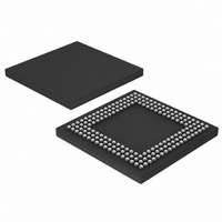
LPC2888FET180/01,5 NXP Semiconductors, LPC2888FET180/01,5 Datasheet - Page 21

LPC2888FET180/01,5
Manufacturer Part Number
LPC2888FET180/01,5
Description
IC ARM7 MCU FLASH 1MB 180TFBGA
Manufacturer
NXP Semiconductors
Series
LPC2800r
Datasheet
1.LPC2888FET180015.pdf
(43 pages)
Specifications of LPC2888FET180/01,5
Core Processor
ARM7
Core Size
16/32-Bit
Speed
60MHz
Connectivity
EBI/EMI, I²C, IrDA, MMC, UART/USART, USB
Peripherals
DMA, I²S, LCD, WDT
Number Of I /o
85
Program Memory Size
1MB (1M x 8)
Program Memory Type
FLASH
Ram Size
64K x 8
Voltage - Supply (vcc/vdd)
1.7 V ~ 3.6 V
Data Converters
A/D 5x10b
Oscillator Type
External
Operating Temperature
-40°C ~ 85°C
Package / Case
180-TFBGA
Processor Series
LPC28
Core
ARM7TDMI-S
Data Bus Width
32 bit
Data Ram Size
64 KB
Interface Type
I2C, I2S, UART, USB
Maximum Clock Frequency
60 MHz
Number Of Programmable I/os
81
Number Of Timers
2
Operating Supply Voltage
1.8 V, 3.3 V
Maximum Operating Temperature
+ 85 C
Mounting Style
SMD/SMT
3rd Party Development Tools
MDK-ARM, RL-ARM, ULINK2
Development Tools By Supplier
OM10092
Minimum Operating Temperature
- 40 C
On-chip Adc
10 bit, 5 Channel
For Use With
OM10092 - EVAL BOARD FOR LPC288X
Lead Free Status / RoHS Status
Lead free / RoHS Compliant
Eeprom Size
-
Lead Free Status / Rohs Status
Details
Other names
568-4528
NXP Semiconductors
LPC2880_LPC2888_3
Preliminary data sheet
6.16.1 Features
6.17.1 Features
6.16 10-bit ADC
6.17 Analog I/O
6.18 USB 2.0 Hi-Speed device controller
The LPC2880/2888 contains a single 10-bit successive approximation ADC with five
multiplexed channels.
The analog I/O system includes an I
dual ADC, and a dual DAC. Each channel includes a separate 4-sample FIFO.
Each of the two ADC inputs is connected to a Programmable Gain Amplifier (PGA).
Each DAC has two output pins.
The USB is a 4-wire bus that supports communication between a host and a number (127
maximum) of peripherals. The host controller allocates the USB bandwidth to attached
devices through a token based protocol. The bus supports hot plugging, un-plugging and
dynamic configuration of the devices. All transactions are initiated by the host controller.
The host schedules transactions in 1 ms frames. Each frame contains an SOF marker and
transactions that transfer data to/from device endpoints. There are four types of transfers
defined for the endpoints. Control transfers are used to configure the device. Interrupt
transfers are used for periodic data transfer. Bulk transfers are used when rate of transfer
is not critical. Isochronous transfers have guaranteed delivery time but no error correction.
•
•
•
•
•
•
•
•
•
•
•
•
•
Serial clock synchronization allows devices with different bit rates to communicate via
one serial bus.
Serial clock synchronization can be used as a handshake mechanism to suspend and
resume serial transfer.
Supports normal (100 kHz) and fast (400 kHz) operation.
10-bit successive approximation ADC.
Input multiplexing among 5 pins.
Power-down mode.
Measurement range 0 V to 3.3 V.
10-bit conversion time
Single or continuous conversion mode.
I
I
Dual 16-bit ADCs with individual inputs routed through programmable gain amplifiers.
Input takes place through a 4-sample FIFO.
Dual 16-bit DACs. Each DAC has its own output pin. Output takes place through a
4-sample FIFO.
2
2
S-bus input channel with a 4-sample FIFO for stereo DAI.
S-bus output channel with a 4-sample FIFO for stereo DAO.
16/32-bit ARM microcontrollers with external memory interface
Rev. 03 — 17 April 2008
2.44 s.
2
S-bus input channel, an I
LPC2880; LPC2888
2
S-bus output channel, a
© NXP B.V. 2008. All rights reserved.
21 of 43


