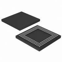
LPC2888FET180/01,5 NXP Semiconductors, LPC2888FET180/01,5 Datasheet - Page 17

LPC2888FET180/01,5
Manufacturer Part Number
LPC2888FET180/01,5
Description
IC ARM7 MCU FLASH 1MB 180TFBGA
Manufacturer
NXP Semiconductors
Series
LPC2800r
Datasheet
1.LPC2888FET180015.pdf
(43 pages)
Specifications of LPC2888FET180/01,5
Core Processor
ARM7
Core Size
16/32-Bit
Speed
60MHz
Connectivity
EBI/EMI, I²C, IrDA, MMC, UART/USART, USB
Peripherals
DMA, I²S, LCD, WDT
Number Of I /o
85
Program Memory Size
1MB (1M x 8)
Program Memory Type
FLASH
Ram Size
64K x 8
Voltage - Supply (vcc/vdd)
1.7 V ~ 3.6 V
Data Converters
A/D 5x10b
Oscillator Type
External
Operating Temperature
-40°C ~ 85°C
Package / Case
180-TFBGA
Processor Series
LPC28
Core
ARM7TDMI-S
Data Bus Width
32 bit
Data Ram Size
64 KB
Interface Type
I2C, I2S, UART, USB
Maximum Clock Frequency
60 MHz
Number Of Programmable I/os
81
Number Of Timers
2
Operating Supply Voltage
1.8 V, 3.3 V
Maximum Operating Temperature
+ 85 C
Mounting Style
SMD/SMT
3rd Party Development Tools
MDK-ARM, RL-ARM, ULINK2
Development Tools By Supplier
OM10092
Minimum Operating Temperature
- 40 C
On-chip Adc
10 bit, 5 Channel
For Use With
OM10092 - EVAL BOARD FOR LPC288X
Lead Free Status / RoHS Status
Lead free / RoHS Compliant
Eeprom Size
-
Lead Free Status / Rohs Status
Details
Other names
568-4528
NXP Semiconductors
LPC2880_LPC2888_3
Preliminary data sheet
6.7.1 Features
6.8.1 Features
6.7 GPIO
6.8 Interrupt controller
Remark: Synchronous static memory devices (synchronous burst mode) are not
supported.
Many device pins that are not needed for a specific peripheral function can be used as
GPIOs. These pins can be controlled by the mode registers. Pins may be dynamically
configured as inputs or outputs. Separate registers allow setting or clearing any number of
outputs simultaneously. The current state of the port pins may be read back via the PIN
registers.
The interrupt controller accepts all of the interrupt request inputs and categorizes them as
FIQ or IRQ. The programmable assignment scheme means that priorities of interrupts
from the various peripherals can be dynamically assigned and adjusted.
FIQ has the highest priority. If more than one request is assigned to FIQ, the interrupt
controller combines the requests to produce the FIQ signal to the ARM processor.
The interrupt controller combines the requests from all the vectored IRQs to produce the
IRQ signal to the ARM processor. The IRQ service routine can start by reading a register
from the interrupt controller and jumping there.
•
•
•
•
•
•
•
•
•
•
•
•
– 2 MB address range with three chip selects.
One chip select for synchronous memory and three chip selects for static memory
devices.
Power-saving modes dynamically control CKE and CLKOUT to SDRAMs.
Dynamic memory self-refresh mode controlled by software.
Controller supports 2048, 4096, and 8192 row address synchronous memory parts.
That is typically 512 MB, 256 MB, and 128 MB parts, with 4, 8, or 16 data lines per
device.
81 pins have dual use as a specific function I/O or as a GPIO.
Each dual use pin can be programmed for functional I/O, drive high, drive low, or
hi-Z/input.
Four pins are dedicated as GPIO, programmable for drive high, drive low, or
hi-Z/input.
Maps all LPC2880/2888 interrupt sources to processor FIQ and IRQ
Level sensitive sources
Programmable priority among sources
Nested interrupt capability
Software interrupt capability for each source
16/32-bit ARM microcontrollers with external memory interface
Rev. 03 — 17 April 2008
LPC2880; LPC2888
© NXP B.V. 2008. All rights reserved.
17 of 43


