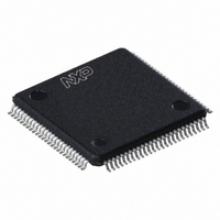
LPC2157FBD100,551 NXP Semiconductors, LPC2157FBD100,551 Datasheet - Page 8

LPC2157FBD100,551
Manufacturer Part Number
LPC2157FBD100,551
Description
IC ARM7 MCU FLASH 512K 100LQFP
Manufacturer
NXP Semiconductors
Series
LPC2100r
Datasheet
1.LPC2157FBD100551.pdf
(45 pages)
Specifications of LPC2157FBD100,551
Program Memory Type
FLASH
Program Memory Size
512KB (512K x 8)
Package / Case
100-LQFP
Core Processor
ARM7
Core Size
16/32-Bit
Speed
60MHz
Connectivity
I²C, Microwire, SPI, SSI, SSP, UART/USART
Peripherals
Brown-out Detect/Reset, LCD, POR, PWM, WDT
Number Of I /o
38
Ram Size
32K x 8
Voltage - Supply (vcc/vdd)
3 V ~ 3.6 V
Data Converters
A/D 16x10b; D/A 1x10b
Oscillator Type
Internal
Operating Temperature
-40°C ~ 85°C
Processor Series
LPC21
Core
ARM7TDMI-S
Data Bus Width
16 bit, 32 bit
Data Ram Size
40 KB
Interface Type
I2C/SPI
Maximum Clock Frequency
60 MHz
Number Of Programmable I/os
38
Number Of Timers
2
Operating Supply Voltage
2.4 V to 3.6 V
Maximum Operating Temperature
+ 85 C
Mounting Style
SMD/SMT
3rd Party Development Tools
MDK-ARM, RL-ARM, ULINK2
Minimum Operating Temperature
- 40 C
On-chip Adc
8-ch x 10-bit
On-chip Dac
1-ch x 10-bit
Lead Free Status / RoHS Status
Lead free / RoHS Compliant
For Use With
568-4310 - EVAL BOARD LPC2158 W/LCD568-4297 - BOARD EVAL LPC21XX MCB2100622-1005 - USB IN-CIRCUIT PROG ARM7 LPC2K
Eeprom Size
-
Lead Free Status / Rohs Status
Lead free / RoHS Compliant
Other names
568-4524
935287348551
935287348551
Available stocks
Company
Part Number
Manufacturer
Quantity
Price
Company:
Part Number:
LPC2157FBD100,551
Manufacturer:
NXP Semiconductors
Quantity:
10 000
NXP Semiconductors
Table 2.
LPC2157_2158_1
Product data sheet
Symbol
P0[27]/AD0[0]/
CAP0[1]/MAT0[1]
P0[28]/AD0[1]/
CAP0[2]/MAT0[2]
P0[29]/AD0[2]/
CAP0[3]/MAT0[3]
P0[30]/AD0[3]/
EINT3/CAP0[0]
P0[31]
P1[0] to P1[31]
P1[16]
P1[17]
P1[25]/EXTIN0
P1[26]/RTCK
P1[27]/TDO
P1[28]/TDI
P1[29]/TCK
P1[30]/TMS
P1[31]/TRST
Pin description LPC2157
Pin
99
1
2
3
5
4
100
16
12
90
86
82
78
8
[4]
[4]
[4]
[6]
[6]
[6]
[7]
[6]
[6]
[6]
[6]
[6]
[6]
[6]
Type
I/O
I
I
O
I/O
I
I
O
I/O
I
I
O
I/O
I
I
I
O
I/O
I/O
I/O
I/O
I
I/O
I/O
I/O
O
I/O
I
I/O
I
I/O
I
I/O
I
…continued
Description
P0[27] — General purpose input/output digital pin (GPIO).
AD0[0] — ADC 0, input 0. This analog input is always connected to its pin.
CAP0[1] — Capture input for Timer 0, channel 1.
MAT0[1] — Match output for Timer 0, channel 1.
P0[28] — General purpose input/output digital pin (GPIO).
AD0[1] — ADC 0, input 1.
CAP0[2] — Capture input for Timer 0, channel 2.
MAT0[2] — Match output for Timer 0, channel 2.
P0[29] — General purpose input/output digital pin (GPIO).
AD0[2] — ADC 0, input 2.
CAP0[3] — Capture input for Timer 0, channel 3.
MAT0[3] — Match output for Timer 0, channel 3.
P0[30] — General purpose input/output digital pin (GPIO).
AD0[3] — ADC 0, input 3.
EINT3 — External interrupt 3 input.
CAP0[0] — Capture input for Timer 0, channel 0.
P0[31] — General purpose output only digital pin.
Port 1: Port 1 is a 32-bit bidirectional I/O port with individual direction controls
for each bit. The operation of port 1 pins depends upon the pin function
selected via the pin connect block. Pins 0 through 15 and 18 through 24 of
port 1 are not available.
P1[16] — General purpose input/output digital pin (GPIO).
P1[17] — General purpose input/output digital pin (GPIO).
P1[25] — General purpose input/output digital pin (GPIO).
EXTIN0 — External Trigger Input. Standard I/O with internal pull-up.
P1[26] — General purpose input/output digital pin (GPIO).
RTCK — Returned Test Clock output. Extra signal added to the JTAG port.
Assists debugger synchronization when processor frequency varies.
Bidirectional pin with internal pull-up.
Note: LOW on RTCK while RESET is LOW enables pins P1[31:26] to operate
as Debug port after reset.
P1[27] — General purpose input/output digital pin (GPIO).
TDO — Test Data out for JTAG interface.
P1[28] — General purpose input/output digital pin (GPIO).
TDI — Test Data in for JTAG interface.
P1[29] — General purpose input/output digital pin (GPIO).
TCK — Test Clock for JTAG interface.
P1[30] — General purpose input/output digital pin (GPIO).
TMS — Test Mode Select for JTAG interface.
P1[31] — General purpose input/output digital pin (GPIO).
TRST — Test Reset for JTAG interface.
Rev. 01 — 15 October 2008
Single-chip 16-bit/32-bit microcontrollers
LPC2157/2158
© NXP B.V. 2008. All rights reserved.
8 of 45


