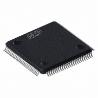
LPC2366FBD100,551 NXP Semiconductors, LPC2366FBD100,551 Datasheet - Page 32

LPC2366FBD100,551
Manufacturer Part Number
LPC2366FBD100,551
Description
IC ARM7 MCU FLASH 256K 100LQFP
Manufacturer
NXP Semiconductors
Series
LPC2300r
Datasheet
1.LPC2364FBD100551.pdf
(59 pages)
Specifications of LPC2366FBD100,551
Program Memory Type
FLASH
Program Memory Size
256KB (256K x 8)
Package / Case
100-LQFP
Core Processor
ARM7
Core Size
16/32-Bit
Speed
72MHz
Connectivity
CAN, Ethernet, I²C, Microwire, SPI, SSI, SSP, UART/USART, USB
Peripherals
Brown-out Detect/Reset, DMA, I²S, POR, PWM, WDT
Number Of I /o
70
Ram Size
58K x 8
Voltage - Supply (vcc/vdd)
3 V ~ 3.6 V
Data Converters
A/D 6x10b; D/A 1x10b
Oscillator Type
Internal
Operating Temperature
-40°C ~ 85°C
Processor Series
LPC23
Core
ARM7TDMI-S
Data Bus Width
16 bit, 32 bit
Data Ram Size
58 KB
Interface Type
CAN/I2C/I2S/SPI/SSP/UART/USB
Maximum Clock Frequency
72 MHz
Number Of Programmable I/os
70
Number Of Timers
4
Operating Supply Voltage
3.3 V
Maximum Operating Temperature
+ 85 C
Mounting Style
SMD/SMT
3rd Party Development Tools
MDK-ARM, RL-ARM, ULINK2
Minimum Operating Temperature
- 40 C
On-chip Adc
6-ch x 10-bit
On-chip Dac
1-ch x 10-bit
Cpu Family
LPC2000
Device Core
ARM7TDMI-S
Device Core Size
16/32Bit
Frequency (max)
72MHz
Total Internal Ram Size
58KB
# I/os (max)
70
Number Of Timers - General Purpose
4
Operating Supply Voltage (typ)
3.3V
Operating Supply Voltage (max)
3.6V
Operating Supply Voltage (min)
3V
Instruction Set Architecture
RISC
Operating Temp Range
-40C to 85C
Operating Temperature Classification
Industrial
Mounting
Surface Mount
Pin Count
100
Package Type
LQFP
Lead Free Status / RoHS Status
Lead free / RoHS Compliant
For Use With
568-4310 - EVAL BOARD LPC2158 W/LCDMCB2360UME - BOARD EVAL MCB2360 + ULINK-MEMCB2360U - BOARD EVAL MCB2360 + ULINK2568-4014 - BOARD EVAL FOR LPC236X ARM568-3999 - BOARD EVAL FOR LPC23 ARM MCU622-1005 - USB IN-CIRCUIT PROG ARM7 LPC2K
Eeprom Size
-
Lead Free Status / Rohs Status
Compliant
Other names
568-3996
935282462551
LPC2366FBD100-S
935282462551
LPC2366FBD100-S
Available stocks
Company
Part Number
Manufacturer
Quantity
Price
Company:
Part Number:
LPC2366FBD100,551
Manufacturer:
NXP Semiconductors
Quantity:
10 000
NXP Semiconductors
LPC2364_65_66_67_68_6
Product data sheet
7.24.4.3 Power-down mode
7.24.4.4 Deep power-down mode
7.24.4.5 Power domains
On the wake-up of Sleep mode, if the IRC was used before entering Sleep mode, the
code execution and peripherals activities will resume after 4 cycles expire. If the main
external oscillator was used, the code execution will resume when 4096 cycles expire.
The customers need to reconfigure the PLL and clock dividers accordingly.
Power-down mode does everything that Sleep mode does, but also turns off the IRC
oscillator and the flash memory. This saves more power, but requires waiting for
resumption of flash operation before execution of code or data access in the flash memory
can be accomplished.
On the wake-up of Power-down mode, if the IRC was used before entering Power-down
mode, it will take IRC 60 μs to start-up. After this 4 IRC cycles will expire before the code
execution can then be resumed if the code was running from SRAM. In the meantime, the
flash wake-up timer then counts 4 MHz IRC clock cycles to make the 100 μs flash start-up
time. When it times out, access to the flash will be allowed. The customers need to
reconfigure the PLL and clock dividers accordingly.
Deep power-down mode is similar to the Power-down mode, but now the on-chip
regulator that supplies power to the internal logic is also shut off. This produces the lowest
possible power consumption without removing power from the entire chip. Since the Deep
power-down mode shuts down the on-chip logic power supply, there is no register or
memory retention, and resumption of operation involves the same activities as a full chip
reset.
If power is supplied to the LPC2364/65/66/67/68 during Deep power-down mode,
wake-up can be caused by the RTC Alarm interrupt or by external Reset.
While in Deep power-down mode, external device power may be removed. In this case,
the LPC2364/65/66/67/68 will start up when external power is restored.
Essential data may be retained through Deep power-down mode (or through complete
powering off of the chip) by storing data in the Battery RAM, as long as the external power
to the VBAT pin is maintained.
The LPC2364/65/66/67/68 provides two independent power domains that allow the bulk
of the device to have power removed while maintaining operation of the RTC and the
battery RAM.
On the LPC2364/65/66/67/68, I/O pads are powered by the 3.3 V (V
the V
power to the CPU and most of the peripherals.
Depending on the LPC2364/65/66/67/68 application, a design can use two power options
to manage power consumption.
DD(DCDC)(3V3)
pin powers the on-chip DC-to-DC converter which in turn provides
Rev. 06 — 1 February 2010
LPC2364/65/66/67/68
Single-chip 16-bit/32-bit microcontrollers
DD(3V3)
© NXP B.V. 2010. All rights reserved.
) pins, while
32 of 59


