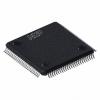
LPC2366FBD100,551 NXP Semiconductors, LPC2366FBD100,551 Datasheet - Page 28

LPC2366FBD100,551
Manufacturer Part Number
LPC2366FBD100,551
Description
IC ARM7 MCU FLASH 256K 100LQFP
Manufacturer
NXP Semiconductors
Series
LPC2300r
Datasheet
1.LPC2364FBD100551.pdf
(59 pages)
Specifications of LPC2366FBD100,551
Program Memory Type
FLASH
Program Memory Size
256KB (256K x 8)
Package / Case
100-LQFP
Core Processor
ARM7
Core Size
16/32-Bit
Speed
72MHz
Connectivity
CAN, Ethernet, I²C, Microwire, SPI, SSI, SSP, UART/USART, USB
Peripherals
Brown-out Detect/Reset, DMA, I²S, POR, PWM, WDT
Number Of I /o
70
Ram Size
58K x 8
Voltage - Supply (vcc/vdd)
3 V ~ 3.6 V
Data Converters
A/D 6x10b; D/A 1x10b
Oscillator Type
Internal
Operating Temperature
-40°C ~ 85°C
Processor Series
LPC23
Core
ARM7TDMI-S
Data Bus Width
16 bit, 32 bit
Data Ram Size
58 KB
Interface Type
CAN/I2C/I2S/SPI/SSP/UART/USB
Maximum Clock Frequency
72 MHz
Number Of Programmable I/os
70
Number Of Timers
4
Operating Supply Voltage
3.3 V
Maximum Operating Temperature
+ 85 C
Mounting Style
SMD/SMT
3rd Party Development Tools
MDK-ARM, RL-ARM, ULINK2
Minimum Operating Temperature
- 40 C
On-chip Adc
6-ch x 10-bit
On-chip Dac
1-ch x 10-bit
Cpu Family
LPC2000
Device Core
ARM7TDMI-S
Device Core Size
16/32Bit
Frequency (max)
72MHz
Total Internal Ram Size
58KB
# I/os (max)
70
Number Of Timers - General Purpose
4
Operating Supply Voltage (typ)
3.3V
Operating Supply Voltage (max)
3.6V
Operating Supply Voltage (min)
3V
Instruction Set Architecture
RISC
Operating Temp Range
-40C to 85C
Operating Temperature Classification
Industrial
Mounting
Surface Mount
Pin Count
100
Package Type
LQFP
Lead Free Status / RoHS Status
Lead free / RoHS Compliant
For Use With
568-4310 - EVAL BOARD LPC2158 W/LCDMCB2360UME - BOARD EVAL MCB2360 + ULINK-MEMCB2360U - BOARD EVAL MCB2360 + ULINK2568-4014 - BOARD EVAL FOR LPC236X ARM568-3999 - BOARD EVAL FOR LPC23 ARM MCU622-1005 - USB IN-CIRCUIT PROG ARM7 LPC2K
Eeprom Size
-
Lead Free Status / Rohs Status
Compliant
Other names
568-3996
935282462551
LPC2366FBD100-S
935282462551
LPC2366FBD100-S
Available stocks
Company
Part Number
Manufacturer
Quantity
Price
Company:
Part Number:
LPC2366FBD100,551
Manufacturer:
NXP Semiconductors
Quantity:
10 000
NXP Semiconductors
LPC2364_65_66_67_68_6
Product data sheet
7.21.1 Features
7.22.1 Features
7.22 Watchdog timer
Three match registers can be used to provide a PWM output with both edges controlled.
Again, the PWMMR0 match register controls the PWM cycle rate. The other match
registers control the two PWM edge positions. Additional double edge controlled PWM
outputs require only two match registers each, since the repetition rate is the same for all
PWM outputs.
With double edge controlled PWM outputs, specific match registers control the rising and
falling edge of the output. This allows both positive going PWM pulses (when the rising
edge occurs prior to the falling edge), and negative going PWM pulses (when the falling
edge occurs prior to the rising edge).
The purpose of the watchdog is to reset the microcontroller within a reasonable amount of
time if it enters an erroneous state. When enabled, the watchdog will generate a system
reset if the user program fails to ‘feed’ (or reload) the watchdog within a predetermined
amount of time.
•
•
•
•
•
•
•
•
•
•
•
LPC2364/65/66/67/68 has one PWM block with Counter or Timer operation (may use
the peripheral clock or one of the capture inputs as the clock source).
Seven match registers allow up to 6 single edge controlled or 3 double edge
controlled PWM outputs, or a mix of both types. The match registers also allow:
– Continuous operation with optional interrupt generation on match.
– Stop timer on match with optional interrupt generation.
– Reset timer on match with optional interrupt generation.
Supports single edge controlled and/or double edge controlled PWM outputs. Single
edge controlled PWM outputs all go high at the beginning of each cycle unless the
output is a constant low. Double edge controlled PWM outputs can have either edge
occur at any position within a cycle. This allows for both positive going and negative
going pulses.
Pulse period and width can be any number of timer counts. This allows complete
flexibility in the trade-off between resolution and repetition rate. All PWM outputs will
occur at the same repetition rate.
Double edge controlled PWM outputs can be programmed to be either positive going
or negative going pulses.
Match register updates are synchronized with pulse outputs to prevent generation of
erroneous pulses. Software must ‘release’ new match values before they can become
effective.
May be used as a standard timer if the PWM mode is not enabled.
A 32-bit Timer/Counter with a programmable 32-bit Prescaler.
Internally resets chip if not periodically reloaded.
Debug mode.
Enabled by software but requires a hardware reset or a watchdog reset/interrupt to be
disabled.
Rev. 06 — 1 February 2010
LPC2364/65/66/67/68
Single-chip 16-bit/32-bit microcontrollers
© NXP B.V. 2010. All rights reserved.
28 of 59


