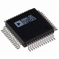
ADUC843BSZ62-5 Analog Devices Inc, ADUC843BSZ62-5 Datasheet - Page 48

ADUC843BSZ62-5
Manufacturer Part Number
ADUC843BSZ62-5
Description
IC ADC 12BIT W/FLASH MCU 52-MQFP
Manufacturer
Analog Devices Inc
Series
MicroConverter® ADuC8xxr
Datasheet
1.EVAL-ADUC842QS.pdf
(88 pages)
Specifications of ADUC843BSZ62-5
Core Size
8-Bit
Program Memory Size
62KB (62K x 8)
Oscillator Type
Internal
Core Processor
8052
Speed
16.78MHz
Connectivity
I²C, SPI, UART/USART
Peripherals
DMA, PSM, PWM, Temp Sensor, WDT
Number Of I /o
32
Program Memory Type
FLASH
Ram Size
2.25K x 8
Voltage - Supply (vcc/vdd)
4.75 V ~ 5.25 V
Data Converters
A/D 8x12b
Operating Temperature
-40°C ~ 85°C
Package / Case
52-MQFP, 52-PQFP
Controller Family/series
(8052) ADUC
No. Of I/o's
34
Ram Memory Size
2KB
Cpu Speed
16.78MHz
No. Of Timers
3
No. Of Pwm
RoHS Compliant
Package
52MQFP
Device Core
8052
Family Name
ADuC8xx
Maximum Speed
16.78 MHz
Operating Supply Voltage
5 V
Data Bus Width
8 Bit
Number Of Programmable I/os
34
Interface Type
I2C/SPI/UART
On-chip Adc
8-chx12-bit
On-chip Dac
2-chx12-bit
Number Of Timers
3
Lead Free Status / RoHS Status
Lead free / RoHS Compliant
Eeprom Size
-
Lead Free Status / RoHS Status
Lead free / RoHS Compliant
Available stocks
Company
Part Number
Manufacturer
Quantity
Price
Company:
Part Number:
ADUC843BSZ62-5
Manufacturer:
AD
Quantity:
1 091
Company:
Part Number:
ADUC843BSZ62-5
Manufacturer:
ADI
Quantity:
170
Company:
Part Number:
ADUC843BSZ62-5
Manufacturer:
Analog Devices Inc
Quantity:
10 000
ADuC841/ADuC842/ADuC843
I
The ADuC841/ADuC842/ADuC843 support a fully licensed
I
hardware slave and software master. SDATA is the data I/O pin,
and SCLOCK is the serial clock. These two pins are shared with
the MOSI and SCLOCK pins of the on-chip SPI interface. To
enable the I
(see SPE in Table 18) or the SPI interface must be moved to
P3.3, P3.4, and P3.5 via the CFG841.1/CFG842.1 bit. Application
Note uC001 describes the operation of this interface as imple-
mented and is available from the MicroConverter website at
www.analog.com/microconverter.
Table 19. I2CCON SFR Bit Designations, Master Mode
Bit No.
7
6
5
4
3
2
1
0
Table 20. I2CCON SFR Bit Designations, Slave Mode
Bit No.
7
6
5
4
3
2
2
C serial interface. The I
C COMPATIBLE INTERFACE
Name
MDO
MDE
MCO
MDI
I2CM
----
----
----
Name
I2CSI
I2CGC
I2CID1
I2CID0
I2CM
2
C interface, the SPI interface must be turned off
Description
I
This data bit is used to implement a master I
the SDATA pin if the data output enable (MDE) bit is set.
I
Set by the user to enable the SDATA pin as an output (Tx).
Cleared by the user to enable the SDATA pin as an input (Rx).
I
This data bit is used to implement a master I
the SCLOCK pin.
I
This data bit is used to implement a master I
this bit on SCLOCK if the data output enable (MDE) bit is 0.
I
Set by the user to enable I
Cleared by the user to enable I
Reserved.
Reserved.
Reserved.
Description
I
Set by the user to enable I
interrupt.
Cleared by the user to disable I
I
Set by hardware after receiving a general call address.
Cleared by the user.
I
Set by hardware to indicate the source of an I
00 Start and Matching Address.
01 Repeated Start and Matching Address.
10 User Data.
11 Stop after a Start and Matching Address.
I
Set by the user to enable I
Cleared by the user to enable I
2
2
2
2
2
2
2
2
2
C Software Master Data Output Bit (Master Mode Only).
C Software Master Data Output Enable Bit (Master Mode Only).
C Software Master Clock Output Bit (Master Mode Only).
C Software Master Data Input Bit (Master Mode Only).
C Master/Slave Mode Bit.
C Stop Interrupt Enable Bit.
C General Call Status Bit.
C Interrupt Decode Bits.
C Master/Slave Mode Bit.
2
C interface is implemented as a full
2
2
2
C software master mode.
C stop interrupts. If set, a stop bit that follows a valid start condition generates an
C software master mode.
2
2
2
C hardware slave mode.
C hardware slave mode.
C stop interrupts.
Rev. 0 | Page 48 of 88
2
2
2
C transmitter interface in software. Data written to this bit is output on
C transmitter interface in software. Data written to this bit is output on
C receiver interface in software. Data on the SDATA pin is latched into
2
C interrupt.
Three SFRs are used to control the I
described in the following tables.
I2CCON
SFR Address
Power-On Default
Bit Addressable
I
E8H
00H
Yes
2
C Control Register
2
C interface and are


