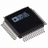
ADUC843BSZ62-5 Analog Devices Inc, ADUC843BSZ62-5 Datasheet - Page 39

ADUC843BSZ62-5
Manufacturer Part Number
ADUC843BSZ62-5
Description
IC ADC 12BIT W/FLASH MCU 52-MQFP
Manufacturer
Analog Devices Inc
Series
MicroConverter® ADuC8xxr
Datasheet
1.EVAL-ADUC842QS.pdf
(88 pages)
Specifications of ADUC843BSZ62-5
Core Size
8-Bit
Program Memory Size
62KB (62K x 8)
Oscillator Type
Internal
Core Processor
8052
Speed
16.78MHz
Connectivity
I²C, SPI, UART/USART
Peripherals
DMA, PSM, PWM, Temp Sensor, WDT
Number Of I /o
32
Program Memory Type
FLASH
Ram Size
2.25K x 8
Voltage - Supply (vcc/vdd)
4.75 V ~ 5.25 V
Data Converters
A/D 8x12b
Operating Temperature
-40°C ~ 85°C
Package / Case
52-MQFP, 52-PQFP
Controller Family/series
(8052) ADUC
No. Of I/o's
34
Ram Memory Size
2KB
Cpu Speed
16.78MHz
No. Of Timers
3
No. Of Pwm
RoHS Compliant
Package
52MQFP
Device Core
8052
Family Name
ADuC8xx
Maximum Speed
16.78 MHz
Operating Supply Voltage
5 V
Data Bus Width
8 Bit
Number Of Programmable I/os
34
Interface Type
I2C/SPI/UART
On-chip Adc
8-chx12-bit
On-chip Dac
2-chx12-bit
Number Of Timers
3
Lead Free Status / RoHS Status
Lead free / RoHS Compliant
Eeprom Size
-
Lead Free Status / RoHS Status
Lead free / RoHS Compliant
Available stocks
Company
Part Number
Manufacturer
Quantity
Price
Company:
Part Number:
ADUC843BSZ62-5
Manufacturer:
AD
Quantity:
1 091
Company:
Part Number:
ADUC843BSZ62-5
Manufacturer:
ADI
Quantity:
170
Company:
Part Number:
ADUC843BSZ62-5
Manufacturer:
Analog Devices Inc
Quantity:
10 000
Using the DAC
The on-chip DAC architecture consists of a resistor string DAC
followed by an output buffer amplifier, the functional equivalent
of which is illustrated in Figure 42. Details of the actual DAC
architecture can be found in U.S. Patent Number 5969657
(www.uspto.gov). Features of this architecture include inherent
guaranteed monotonicity and excellent differential linearity.
As shown in Figure 42, the reference source for each DAC is
user selectable in software. It can be either AV
0 V-to-AV
from 0 V to the voltage at the AV
the DAC output transfer function spans from 0 V to the internal
V
pin. The DAC output buffer amplifier features a true rail-to-rail
output stage implementation. This means that unloaded, each
output is capable of swinging to within less than 100 mV of
both AVDD and ground. Moreover, the DAC’s linearity specifica-
tion (when driving a 10 kΩ resistive load to ground) is guaranteed
through the full transfer function except Codes 0 to 100, and, in
0 V-to-AVDD mode only, Codes 3995 to 4095. Linearity degrada-
tion near ground and V
amplifier, and a general representation of its effects (neglecting
offset and gain error) is illustrated in Figure 43. The dotted line
in Figure 43 indicates the ideal transfer function, and the solid
line represents what the transfer function might look like with
endpoint nonlinearities due to saturation of the output amplifier.
Note that Figure 43 represents a transfer function in 0 V-to-V
mode only. In 0 V-to-V
nonlinearity would be similar, but the upper portion of the
transfer function would follow the ideal line right to the end
(V
linearity errors.
REF
REF
or, if an external reference is applied, the voltage at the C
in this case, not V
AV
V
DD
Figure 42. Resistor String DAC Functional Equivalent
REF
DD
mode, the DAC output transfer function spans
ADuC841/ADuC842
R
R
R
R
R
REF
DD
DD
), showing no signs of endpoint
mode (with V
is caused by saturation of the output
DD
(FROM MCU)
pin. In 0 V-to-V
DISABLE
OUTPUT
BUFFER
HIGH Z
REF
< V
DD
DD
or V
), the lower
DAC0
REF
REF
mode,
. In
Rev. 0 | Page 39 of 88
DD
REF
V
V
DD
DD
–100mV
–50mV
100mV
50mV
Figure 44. Source and Sink Current Capability with V
Figure 45. Source and Sink Current Capability with V
0mV
V
Figure 43. Endpoint Nonlinearities Due to Amplifier Saturation
DD
4
3
1
0
5
4
3
2
1
0
0
0
000H
DAC LOADED WITH 0FFFH
DAC LOADED WITH 0000H
ADuC841/ADuC842/ADuC843
SOURCE/SINK CURRENT (mA)
SOURCE/SINK CURRENT (mA)
5
5
DAC LOADED WITH 0FFFH
DAC LOADED WITH 0000H
10
10
REF
REF
= V
= V
DD
DD
= 5 V
= 3 V
15
15
FFFH


