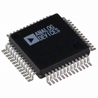
ADUC843BSZ62-5 Analog Devices Inc, ADUC843BSZ62-5 Datasheet - Page 47

ADUC843BSZ62-5
Manufacturer Part Number
ADUC843BSZ62-5
Description
IC ADC 12BIT W/FLASH MCU 52-MQFP
Manufacturer
Analog Devices Inc
Series
MicroConverter® ADuC8xxr
Datasheet
1.EVAL-ADUC842QS.pdf
(88 pages)
Specifications of ADUC843BSZ62-5
Core Size
8-Bit
Program Memory Size
62KB (62K x 8)
Oscillator Type
Internal
Core Processor
8052
Speed
16.78MHz
Connectivity
I²C, SPI, UART/USART
Peripherals
DMA, PSM, PWM, Temp Sensor, WDT
Number Of I /o
32
Program Memory Type
FLASH
Ram Size
2.25K x 8
Voltage - Supply (vcc/vdd)
4.75 V ~ 5.25 V
Data Converters
A/D 8x12b
Operating Temperature
-40°C ~ 85°C
Package / Case
52-MQFP, 52-PQFP
Controller Family/series
(8052) ADUC
No. Of I/o's
34
Ram Memory Size
2KB
Cpu Speed
16.78MHz
No. Of Timers
3
No. Of Pwm
RoHS Compliant
Package
52MQFP
Device Core
8052
Family Name
ADuC8xx
Maximum Speed
16.78 MHz
Operating Supply Voltage
5 V
Data Bus Width
8 Bit
Number Of Programmable I/os
34
Interface Type
I2C/SPI/UART
On-chip Adc
8-chx12-bit
On-chip Dac
2-chx12-bit
Number Of Timers
3
Lead Free Status / RoHS Status
Lead free / RoHS Compliant
Eeprom Size
-
Lead Free Status / RoHS Status
Lead free / RoHS Compliant
Available stocks
Company
Part Number
Manufacturer
Quantity
Price
Company:
Part Number:
ADUC843BSZ62-5
Manufacturer:
AD
Quantity:
1 091
Company:
Part Number:
ADUC843BSZ62-5
Manufacturer:
ADI
Quantity:
170
Company:
Part Number:
ADUC843BSZ62-5
Manufacturer:
Analog Devices Inc
Quantity:
10 000
Using the SPI Interface
Depending on the configuration of the bits in the SPICON SFR
shown in Table 18, the ADuC841/ADuC842/ADuC843 SPI
interface transmits or receives data in a number of possible
modes. Figure 54 shows all possible SPI configurations for the
parts, and the timing relationships and synchronization
between the signals involved. Also shown in this figure is the
SPI interrupt bit (ISPI) and how it is triggered at the end of each
byte-wide communication.
SPI Interface—Master Mode
In master mode, the SCLOCK pin is always an output and
generates a burst of eight clocks whenever user code writes to
the SPIDAT register. The SCLOCK bit rate is determined by
SPR0 and SPR1 in SPICON. Also note that the SS pin is not
used in master mode. If the parts need to assert the SS pin on an
external slave device, a port digital output pin should be used.
(CPHA = 1)
(CPHA = 0)
SAMPLE INPUT
DATA OUTPUT
SAMPLE INPUT
DATA OUTPUT
(CPOL = 1)
(CPOL = 0)
ISPI FLAG
ISPI FLAG
SCLOCK
SCLOCK
Figure 54. SPI Timing, All Modes
SS
?
MSB BIT 6 BIT 5
MSB BIT 6 BIT 5 BIT 4 BIT 3 BIT 2 BIT 1 LSB
BIT 4 BIT 3 BIT 2 BIT 1 LSB
?
Rev. 0 | Page 47 of 88
In master mode, a byte transmission or reception is initiated by
a write to SPIDAT. Eight clock periods are generated via the
SCLOCK pin and the SPIDAT byte being transmitted via MOSI.
With each SCLOCK period, a data bit is also sampled via MISO.
After eight clocks, the transmitted byte will be completely
transmitted, and the input byte will be waiting in the input shift
register. The ISPI flag will be set automatically, and an interrupt
will occur if enabled. The value in the shift register will be
latched into SPIDAT.
SPI Interface—Slave Mode
In slave mode, SCLOCK is an input. The SS pin must also be
driven low externally during the byte communication. Trans-
mission is also initiated by a write to SPIDAT. In slave mode, a
data bit is transmitted via MISO, and a data bit is received via
MOSI through each input SCLOCK period. After eight clocks,
the transmitted byte will be completely transmitted, and the
input byte will be waiting in the input shift register. The ISPI
flag will be set automatically, and an interrupt will occur if
enabled. The value in the shift register will be latched into
SPIDAT only when the transmission/reception of a byte has
been completed. The end of transmission occurs after the
eighth clock has been received if CPHA = 1, or when SS returns
high if CPHA = 0.
ADuC841/ADuC842/ADuC843


