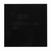
LPC3250FET296/01,5 NXP Semiconductors, LPC3250FET296/01,5 Datasheet - Page 41

LPC3250FET296/01,5
Manufacturer Part Number
LPC3250FET296/01,5
Description
IC ARM9 MCU 256K 296-TFBGA
Manufacturer
NXP Semiconductors
Series
LPC32x0r
Specifications of LPC3250FET296/01,5
Package / Case
296-TFBGA
Core Processor
ARM9
Core Size
16/32-Bit
Speed
266MHz
Connectivity
EBI/EMI, Ethernet, I²C, IrDA, Microwire, SPI, SSI, SSP, UART/USART, USB OTG
Peripherals
DMA, I²S, LCD, Motor Control PWM, PWM, WDT
Number Of I /o
51
Program Memory Type
ROMless
Ram Size
256K x 8
Voltage - Supply (vcc/vdd)
0.9 V ~ 3.6 V
Data Converters
A/D 3x10b
Oscillator Type
Internal
Operating Temperature
-40°C ~ 85°C
Processor Series
LPC32
Core
ARM926EJ-S
Data Bus Width
32 bit
Data Ram Size
256 KB
Interface Type
EMC
Maximum Clock Frequency
266 MHz
Number Of Timers
6
Operating Supply Voltage
1.31 V to 1.39 V
Maximum Operating Temperature
+ 85 C
Mounting Style
SMD/SMT
3rd Party Development Tools
MDK-ARM, RL-ARM, ULINK2, DK-57TS-LPC3250, DK-57VTS-LPC3250, SOMDIMM-LPC3250
Development Tools By Supplier
OM11016, OM11021, OM11045
Minimum Operating Temperature
- 40 C
On-chip Adc
10 bit, 3 Channel
Lead Free Status / RoHS Status
Lead free / RoHS Compliant
Eeprom Size
-
Program Memory Size
-
Lead Free Status / Rohs Status
Lead free / RoHS Compliant
Other names
568-4962
935290766551
935290766551
Available stocks
Company
Part Number
Manufacturer
Quantity
Price
Company:
Part Number:
LPC3250FET296/01,5
Manufacturer:
TI
Quantity:
250
Company:
Part Number:
LPC3250FET296/01,5
Manufacturer:
NXP Semiconductors
Quantity:
10 000
Part Number:
LPC3250FET296/01,5
Manufacturer:
NXP/恩智浦
Quantity:
20 000
NXP Semiconductors
8. Basic architecture
LPC3220_30_40_50_1
Preliminary data sheet
The LPC3220/30/40/50 is a general purpose ARM926EJ-S 32-bit microprocessor with a
32 kB instruction cache and a 32 kB data cache. The microcontroller offers high
performance and very low power consumption. The ARM architecture is based on RISC
principles, which results in the instruction set and related decode mechanism being much
simpler than equivalent micro programmed CISCs. This simplicity results in a high
instruction throughput and impressive real-time interrupt response from a small and
cost-effective processor core.
The ARM926EJ-S core employs a 5-stage pipeline so processing and memory system
accesses can occur continuously. At any one point in time, several operations are in
progress: subsequent instruction fetch, next instruction decode, instruction execution,
memory access, and write-back. The combination of architectural enhancements gives
the ARM9 about 30 % better performance than an ARM7 running at the same clock rate:
The ARM926EJ-S processor also employs an operational state known as Thumb, which
makes it ideally suited to high-volume applications with memory restrictions, or
applications where code density is an issue.
The key idea behind Thumb state is the use of a super-reduced instruction set.
Essentially, the ARM926EJ-S processor core has two instruction sets:
The Thumb set’s smaller 16-bit instruction length allows it to approach twice the density of
standard ARM code while retaining many of ARM’s 32-bit performance advantage over a
traditional 16-bit processor using 16-bit registers. This is possible because Thumb code
operates using the same 32-bit register set as ARM code. Thumb code size is up to 65 %
smaller than ARM code size, and 160 % of the performance of an equivalent ARM
processor connected to a 16-bit memory system. Additionally, the ARM926EJ-S core
includes enhanced DSP instructions and multiplier, as well as an enhanced 32-bit MAC
block.
1. The standard 32-bit ARM set
2. The 16-bit Thumb set
•
•
•
•
•
•
•
32-bit pulse-width (match) register
10-bit dead-time register and an associated 10-bit dead-time counter
32-bit capture register
Two PWM (match) outputs (pins MCOA0/1/2 and MCOB0/1/2) with opposite polarities
Period interrupt, pulse-width interrupt, and capture interrupt
Approximately 1.3 clocks per instruction for the ARM926 compared to 1.9 clocks per
instruction for ARM7TDMI.
Approximately 1.1 Dhrystone MIPS/MHz for the ARM926 compared to 0.9 Dhrystone
MIPS/MHz for ARM7TDMI.
Rev. 01 — 6 February 2009
LPC3220/30/40/50
16/32-bit ARM microcontrollers
© NXP B.V. 2009. All rights reserved.
41 of 73


