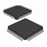
P87C660X2BBD,157 NXP Semiconductors, P87C660X2BBD,157 Datasheet - Page 87

P87C660X2BBD,157
Manufacturer Part Number
P87C660X2BBD,157
Description
IC 80C51 MCU 16K OTP 44-LQFP
Manufacturer
NXP Semiconductors
Series
87Cr
Datasheet
1.P87C660X2BBD157.pdf
(102 pages)
Specifications of P87C660X2BBD,157
Core Processor
8051
Core Size
8-Bit
Speed
33MHz
Connectivity
EBI/EMI, I²C, UART/USART
Peripherals
POR, PWM, WDT
Number Of I /o
32
Program Memory Size
16KB (16K x 8)
Program Memory Type
OTP
Ram Size
512 x 8
Voltage - Supply (vcc/vdd)
2.7 V ~ 5.5 V
Oscillator Type
Internal
Operating Temperature
0°C ~ 70°C
Package / Case
44-LQFP
Processor Series
P87C6x
Core
80C51
Data Bus Width
8 bit
Data Ram Size
512 B
Interface Type
I2C, UART
Maximum Clock Frequency
16 MHz, 33 MHz
Number Of Programmable I/os
32
Number Of Timers
3
Operating Supply Voltage
2.7 V to 5.5 V
Maximum Operating Temperature
+ 70 C
Mounting Style
SMD/SMT
3rd Party Development Tools
PK51, CA51, A51, ULINK2
Minimum Operating Temperature
0 C
Lead Free Status / RoHS Status
Lead free / RoHS Compliant
Eeprom Size
-
Data Converters
-
Lead Free Status / Rohs Status
Details
Other names
568-3204
935273061157
P87C660X2BBD
935273061157
P87C660X2BBD
Available stocks
Company
Part Number
Manufacturer
Quantity
Price
Company:
Part Number:
P87C660X2BBD,157
Manufacturer:
NXP Semiconductors
Quantity:
10 000
1. A device must internally provide a hold time of at least 300 ns for the SDA signal (referred to the V
2. The maximum t
3. A fast mode I
4. C
Philips Semiconductors
I
All values referred to V
NOTES:
2003 Oct 02
2
Symbol
f
t
t
t
t
t
t
t
t
t
t
C
t
SCL
BUF
HD; STA
LOW
HIGH
SU; STA
HD;DAT
SU;DAT
FD
FD
SU; STO
SP
C-BUS INTERFACE TIMING (5 V, 3.5 MHZ TO 16 MHZ) NOT TESTED, GUARANTEED BY DESIGN
b
80C51 8-bit microcontroller family
RAM, low voltage (2.7 to 5.5 V), low power, high speed (30/33
MHz), two 400KB I
the undefined region of the falling edge of SCL.
will automatically be the case if the device does not stretch the LOW period of the SCL signal. If such a device does stretch the LOW period
of the SCL signal, it must output the next data bit to the SDA line t
I
, t
, t
2
b
C-bus specification) before the SCL line is released.
FC
FC
= total capacitance of one bus line in pF.
Figure
2
C-bus device can be used in a standard mode I
HD;DAT
IH(min)
2
C interfaces
Parameter
SCL clock frequency
Bus free time between a STOP and START
condition
Hold time (repeated) START condition. After this
period, the first clock pulse is generated
LOW period of the SCL clock
High period of the SCL clock
Set-up time for a repeated START condition
Data hold time:
– for CBUS compatible masters (notes 1, 3)
– for I
Data set-up time
Rise time of both SDA and SCL signals
Fall time of both SDA and SCL signals
Set-up time for STOP condition
Capacitive load for each bus line
Pulse width of spikes which must be suppressed
by the input filter
has only to be met if the device does not stretch the LOW period (t
and V
2
C–bus devices (notes 1, 2)
IL(max)
levels; see Figure TBD
16 KB OTP/ROM, 512B
2
C-bus system, but the requirement t
R(max)
87
+ t
I
STANDARD MODE
MIN
0
4.7
4.0
4.7
4.0
4.7
5.0
0
250
–
–
4.0
–
–
2
SU<DAT
C-BUS
= 1000 + 250 = 1250 ns (according to the standard-mode
MAX
100
–
–
–
–
–
–
–
–
1000
300
–
400
–
LOW)
of the SCL signal.
IHmin
SU, DAT
FAST MODE
MIN
0
1.3
0.6
1.3
0.6
0.6
–
0
100
20 + 0.1 c
0.6
–
0
of the SCL signal) in order to bridge
P8xC660X2/661X2
3
> 250 ns must then be met. This
b
4
MAX
400
–
–
–
–
–
–
0.9
–
300
–
400
50
Product data
Unit
kHz
ns
ns
pF
ns
s
s
s
s
s
s
s


