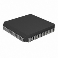
PIC17C752-16/L Microchip Technology, PIC17C752-16/L Datasheet - Page 93

PIC17C752-16/L
Manufacturer Part Number
PIC17C752-16/L
Description
IC MCU OTP 8KX16 A/D PWM 68PLCC
Manufacturer
Microchip Technology
Series
PIC® 17Cr
Datasheets
1.PIC16F616T-ISL.pdf
(8 pages)
2.PIC17C752-16L.pdf
(304 pages)
3.PIC17C752-16L.pdf
(4 pages)
4.PIC17C752-16L.pdf
(6 pages)
Specifications of PIC17C752-16/L
Core Size
8-Bit
Program Memory Size
16KB (8K x 16)
Peripherals
Brown-out Detect/Reset, POR, PWM, WDT
Core Processor
PIC
Speed
16MHz
Connectivity
I²C, SPI, UART/USART
Number Of I /o
50
Program Memory Type
OTP
Ram Size
454 x 8
Voltage - Supply (vcc/vdd)
4.5 V ~ 5.5 V
Data Converters
A/D 12x10b
Oscillator Type
External
Operating Temperature
0°C ~ 70°C
Package / Case
68-PLCC
Controller Family/series
PIC17
No. Of I/o's
50
Ram Memory Size
678Byte
Cpu Speed
16MHz
No. Of Timers
4
Processor Series
PIC17C
Core
PIC
Data Bus Width
8 bit
Data Ram Size
678 B
Interface Type
I2C, MSSP, RS- 232, SCI, SPI, USART
Maximum Clock Frequency
33 MHz
Number Of Programmable I/os
50
Number Of Timers
8
Operating Supply Voltage
3 V to 5.5 V
Maximum Operating Temperature
+ 70 C
Mounting Style
SMD/SMT
Development Tools By Supplier
ICE2000, DM173001
Minimum Operating Temperature
0 C
On-chip Adc
12 bit
Lead Free Status / RoHS Status
Lead free / RoHS Compliant
For Use With
AC164308 - MODULE SKT FOR PM3 68PLCCDVA17XL681 - DEVICE ADAPTER FOR PIC17C752DM173001 - KIT DEVELOPMENT PICDEM17AC174007 - MODULE SKT PROMATEII 68PLCCAC164024 - ADAPTER PICSTART PLUS 68PLCC
Eeprom Size
-
Lead Free Status / Rohs Status
Details
Available stocks
Company
Part Number
Manufacturer
Quantity
Price
Company:
Part Number:
PIC17C752-16/L
Manufacturer:
Microchip
Quantity:
120
Company:
Part Number:
PIC17C752-16/L
Manufacturer:
Microchip Technology
Quantity:
10 000
- PIC16F616T-ISL PDF datasheet
- PIC17C752-16L PDF datasheet #2
- PIC17C752-16L PDF datasheet #3
- PIC17C752-16L PDF datasheet #4
- Current page: 93 of 304
- Download datasheet (6Mb)
10.10 I/O Programming Considerations
10.10.1
Any instruction which writes, operates internally as a
read, followed by a write operation. For example, the
BCF and BSF instructions read the register into the
CPU, execute the bit operation and write the result
back to the register. Caution must be used when these
instructions are applied to a port with both inputs and
outputs defined. For example, a BSF operation on bit5
of PORTB, will cause all eight bits of PORTB to be read
into the CPU. Then the BSF operation takes place on
bit5 and PORTB is written to the output latches. If
another bit of PORTB is used as a bi-directional I/O pin
(e.g. bit0) and it is defined as an input at this time, the
input signal present on the pin itself would be read into
the CPU and rewritten to the data latch of this particular
pin, overwriting the previous content. As long as the pin
stays in the input mode, no problem occurs. However,
if bit0 is switched into output mode later on, the content
of the data latch may now be unknown.
Reading a port reads the values of the port pins. Writing
to the port register writes the value to the port latch.
When using read-modify-write instructions (BCF, BSF,
BTG, etc.) on a port, the value of the port pins is read,
the desired operation is performed with this value and
the value is then written to the port latch.
Example 10-10 shows the possible effect of two
sequential read-modify-write instructions on an I/O port.
2000 Microchip Technology Inc.
BI-DIRECTIONAL I/O PORTS
EXAMPLE 10-10: READ-MODIFY-WRITE
; Initial PORT settings: PORTB<7:4> Inputs
;
; PORTB<7:6> have pull-ups and are
; not connected to other circuitry
;
;
;
;
;
; Note that the user may have expected the
; pin values to be 00pp pppp. The 2nd BCF
; caused RB7 to be latched as the pin value
; (High).
Note:
BCF
BCF
BCF
BCF
A pin actively outputting a Low or High
should not be driven from external devices,
in order to change the level on this pin (i.e.,
“wired-or”, “wired-and”). The resulting high
output currents may damage the device.
PORTB, 7
PORTB, 6
DDRB, 7
DDRB, 6
INSTRUCTIONS ON AN
I/O PORT
PIC17C7XX
; 01pp pppp
; 10pp pppp
; 10pp pppp
; 10pp pppp
PORT latch
----------
PORTB<3:0> Outputs
DS30289B-page 93
PORT pins
---------
11pp pppp
11pp pppp
11pp pppp
10pp pppp
Related parts for PIC17C752-16/L
Image
Part Number
Description
Manufacturer
Datasheet
Request
R

Part Number:
Description:
IC MCU OTP 8KX16 A/D PWM 68PLCC
Manufacturer:
Microchip Technology
Datasheet:

Part Number:
Description:
High-Performance 8-Bit CMOS EPROM Microcontrollers
Manufacturer:
MICROCHIP [Microchip Technology]
Datasheet:

Part Number:
Description:
High-Performance 8-Bit CMOS EPROM Microcontrollers with 10-bit A/D
Manufacturer:
MICROCHIP [Microchip Technology]
Datasheet:

Part Number:
Description:
IC MCU OTP 8KX16 A/D PWM 68PLCC
Manufacturer:
Microchip Technology
Datasheet:

Part Number:
Description:
IC MCU OTP 8KX16 A/D PWM 64TQFP
Manufacturer:
Microchip Technology
Datasheet:

Part Number:
Description:
IC MCU OTP 8KX16 A/D PWM 64TQFP
Manufacturer:
Microchip Technology
Datasheet:

Part Number:
Description:
IC MCU OTP 8KX16 A/D PWM 64TQFP
Manufacturer:
Microchip Technology
Datasheet:

Part Number:
Description:
IC MCU OTP 8KX16 A/D PWM 64TQFP
Manufacturer:
Microchip Technology
Datasheet:

Part Number:
Description:
IC MCU OTP 8KX16 A/D PWM 68PLCC
Manufacturer:
Microchip Technology
Datasheet:

Part Number:
Description:
IC MCU CMOS 33MHZ 8K EPRM 68PLCC
Manufacturer:
Microchip Technology
Datasheet:

Part Number:
Description:
IC MCU CMOS 16MHZ 8K EPRM 68PLCC
Manufacturer:
Microchip Technology
Datasheet:

Part Number:
Description:
IC MCU CMOS 16MHZ 8K EPRM 64TQFP
Manufacturer:
Microchip Technology
Datasheet:

Part Number:
Description:
IC MCU CMOS 33MHZ 8K EPRM 64TQFP
Manufacturer:
Microchip Technology
Datasheet:


