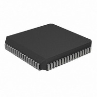
PIC17C752-16/L Microchip Technology, PIC17C752-16/L Datasheet - Page 86

PIC17C752-16/L
Manufacturer Part Number
PIC17C752-16/L
Description
IC MCU OTP 8KX16 A/D PWM 68PLCC
Manufacturer
Microchip Technology
Series
PIC® 17Cr
Datasheets
1.PIC16F616T-ISL.pdf
(8 pages)
2.PIC17C752-16L.pdf
(304 pages)
3.PIC17C752-16L.pdf
(4 pages)
4.PIC17C752-16L.pdf
(6 pages)
Specifications of PIC17C752-16/L
Core Size
8-Bit
Program Memory Size
16KB (8K x 16)
Peripherals
Brown-out Detect/Reset, POR, PWM, WDT
Core Processor
PIC
Speed
16MHz
Connectivity
I²C, SPI, UART/USART
Number Of I /o
50
Program Memory Type
OTP
Ram Size
454 x 8
Voltage - Supply (vcc/vdd)
4.5 V ~ 5.5 V
Data Converters
A/D 12x10b
Oscillator Type
External
Operating Temperature
0°C ~ 70°C
Package / Case
68-PLCC
Controller Family/series
PIC17
No. Of I/o's
50
Ram Memory Size
678Byte
Cpu Speed
16MHz
No. Of Timers
4
Processor Series
PIC17C
Core
PIC
Data Bus Width
8 bit
Data Ram Size
678 B
Interface Type
I2C, MSSP, RS- 232, SCI, SPI, USART
Maximum Clock Frequency
33 MHz
Number Of Programmable I/os
50
Number Of Timers
8
Operating Supply Voltage
3 V to 5.5 V
Maximum Operating Temperature
+ 70 C
Mounting Style
SMD/SMT
Development Tools By Supplier
ICE2000, DM173001
Minimum Operating Temperature
0 C
On-chip Adc
12 bit
Lead Free Status / RoHS Status
Lead free / RoHS Compliant
For Use With
AC164308 - MODULE SKT FOR PM3 68PLCCDVA17XL681 - DEVICE ADAPTER FOR PIC17C752DM173001 - KIT DEVELOPMENT PICDEM17AC174007 - MODULE SKT PROMATEII 68PLCCAC164024 - ADAPTER PICSTART PLUS 68PLCC
Eeprom Size
-
Lead Free Status / Rohs Status
Details
Available stocks
Company
Part Number
Manufacturer
Quantity
Price
Company:
Part Number:
PIC17C752-16/L
Manufacturer:
Microchip
Quantity:
120
Company:
Part Number:
PIC17C752-16/L
Manufacturer:
Microchip Technology
Quantity:
10 000
- PIC16F616T-ISL PDF datasheet
- PIC17C752-16L PDF datasheet #2
- PIC17C752-16L PDF datasheet #3
- PIC17C752-16L PDF datasheet #4
- Current page: 86 of 304
- Download datasheet (6Mb)
PIC17C7XX
10.7
PORTG is an 8-bit wide, bi-directional port. The corre-
sponding data direction register is DDRG. A ’1’ in
DDRG configures the corresponding port pin as an
input. A ’0’ in the DDRG register configures the corre-
sponding port pin as an output. Reading PORTG reads
the status of the pins, whereas writing to PORTG will
write to the port latch.
The lower four bits of PORTG are multiplexed with four
channels of the 10-bit A/D converter.
The remaining bits of PORTG are multiplexed with
peripheral output and inputs. RG4 is multiplexed with
the CAP3 input, RG5 is multiplexed with the PWM3
output, RG6 and RG7 are multiplexed with the
USART2 functions.
Upon RESET, RG3:RG0 is automatically configured as
analog inputs and must be configured in software to be
a digital I/O.
FIGURE 10-14:
DS30289B-page 86
WR PORTG
WR DDRG
RD PORTG
Note: I/O pins have protection diodes to V
V
Data Bus
AIN
PORTG and DDRG Registers
PCFG3:PCFG0
CHS3:CHS0
BLOCK DIAGRAM OF RG3:RG0
Data Latch
DDRG Latch
D
CK
D
CK
RD DDRG
Q
Q
Q
Q
DD
and V
SS
Q
.
EN
EN
D
Example 10-7 shows the instruction sequence to initial-
ize PORTG. The Bank Select Register (BSR) must be
selected to Bank 5 for the port to be initialized. The fol-
lowing example uses the MOVLB instruction to load the
BSR register for bank selection.
EXAMPLE 10-7:
To other pads
To other pads
CLRF
MOVWF
MOVLB
MOVLW
MOVPF
MOVLW
PORTG, F
5
0x0E
WREG, ADCON1
DDRG
0x03
V
V
P
N
DD
SS
INITIALIZING PORTG
2000 Microchip Technology Inc.
; Initialize PORTG data
; Set RG<1:0> as inputs
;
;
; Select Bank 5
; Configure PORTG as
; digital
;
;
; Value used to init
;
the data direction
RG<7:2> as outputs
latches before
register
data direction
ST
Input
Buffer
I/O pin
Related parts for PIC17C752-16/L
Image
Part Number
Description
Manufacturer
Datasheet
Request
R

Part Number:
Description:
IC MCU OTP 8KX16 A/D PWM 68PLCC
Manufacturer:
Microchip Technology
Datasheet:

Part Number:
Description:
High-Performance 8-Bit CMOS EPROM Microcontrollers
Manufacturer:
MICROCHIP [Microchip Technology]
Datasheet:

Part Number:
Description:
High-Performance 8-Bit CMOS EPROM Microcontrollers with 10-bit A/D
Manufacturer:
MICROCHIP [Microchip Technology]
Datasheet:

Part Number:
Description:
IC MCU OTP 8KX16 A/D PWM 68PLCC
Manufacturer:
Microchip Technology
Datasheet:

Part Number:
Description:
IC MCU OTP 8KX16 A/D PWM 64TQFP
Manufacturer:
Microchip Technology
Datasheet:

Part Number:
Description:
IC MCU OTP 8KX16 A/D PWM 64TQFP
Manufacturer:
Microchip Technology
Datasheet:

Part Number:
Description:
IC MCU OTP 8KX16 A/D PWM 64TQFP
Manufacturer:
Microchip Technology
Datasheet:

Part Number:
Description:
IC MCU OTP 8KX16 A/D PWM 64TQFP
Manufacturer:
Microchip Technology
Datasheet:

Part Number:
Description:
IC MCU OTP 8KX16 A/D PWM 68PLCC
Manufacturer:
Microchip Technology
Datasheet:

Part Number:
Description:
IC MCU CMOS 33MHZ 8K EPRM 68PLCC
Manufacturer:
Microchip Technology
Datasheet:

Part Number:
Description:
IC MCU CMOS 16MHZ 8K EPRM 68PLCC
Manufacturer:
Microchip Technology
Datasheet:

Part Number:
Description:
IC MCU CMOS 16MHZ 8K EPRM 64TQFP
Manufacturer:
Microchip Technology
Datasheet:

Part Number:
Description:
IC MCU CMOS 33MHZ 8K EPRM 64TQFP
Manufacturer:
Microchip Technology
Datasheet:


