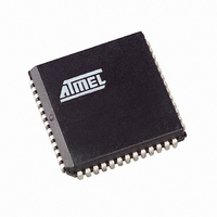
AT89C51CC03C-S3RIM Atmel, AT89C51CC03C-S3RIM Datasheet - Page 44

AT89C51CC03C-S3RIM
Manufacturer Part Number
AT89C51CC03C-S3RIM
Description
IC 8051 MCU FLASH 64K 52PLCC
Manufacturer
Atmel
Series
AT89C CANr
Datasheets
1.AT89C51CC03C-S3RIM.pdf
(198 pages)
2.AT89C51CC03C-S3RIM.pdf
(32 pages)
3.AT89C51CC03C-S3RIM.pdf
(27 pages)
4.AT89C51CC03C-S3RIM.pdf
(184 pages)
Specifications of AT89C51CC03C-S3RIM
Core Processor
8051
Core Size
8-Bit
Speed
40MHz
Connectivity
CAN, SPI, UART/USART
Peripherals
POR, PWM, WDT
Number Of I /o
36
Program Memory Size
64KB (64K x 8)
Program Memory Type
FLASH
Eeprom Size
2K x 8
Ram Size
2.25K x 8
Voltage - Supply (vcc/vdd)
3 V ~ 5.5 V
Data Converters
A/D 8x10b
Oscillator Type
External
Operating Temperature
-40°C ~ 85°C
Package / Case
52-PLCC
Lead Free Status / RoHS Status
Contains lead / RoHS non-compliant
Other names
AT89C51CC03CS3RTR
Available stocks
Company
Part Number
Manufacturer
Quantity
Price
- AT89C51CC03C-S3RIM PDF datasheet
- AT89C51CC03C-S3RIM PDF datasheet #2
- AT89C51CC03C-S3RIM PDF datasheet #3
- AT89C51CC03C-S3RIM PDF datasheet #4
- Current page: 44 of 198
- Download datasheet (3Mb)
FM0 Memory Architecture
User Space
Extra Row (XRow)
Hardware security Byte (HSB)
Column Latches
Cross Flash Memory Access
Description
44
AT89C51CC03
The Flash memory is made up of 4 blocks (see Figure 23):
•
•
•
•
This space is composed of a 64K Bytes Flash memory organized in 512 pages of 128
Bytes. It contains the user’s application code.
This row is a part of FM0 and has a size of 128 Bytes. The extra row may contain infor-
mation for boot loader usage.
The Hardware security Byte space is a part of FM0 and has a size of 1 byte.
The 4 MSB can be read/written by software (from FM0 and , the 4 LSB can only be read
by software and written by hardware in parallel mode.
H Hardware Security Byte (HSB)
The column latches, also part of FM0, have a size of full page (128 Bytes).
The column latches are the entrance buffers of the three previous memory locations
(user array, XROW and Hardware security byte). The column latches are write only and
can be accessed only from FM1 (boot mode) and from external memory
The FM0 memory can be program only from FM1. Programming FM0 from FM0 or from
external memory is impossible.
The FM1 memory can be program only by parallel programming.
The Table show all software Flash access allowed.
Number
Bit
2-0
The memory array (user space) 64K Bytes
The Extra Row
The Hardware security bits
The column latch registers
X2
7
6
5
4
3
7
Mnemonic
LB2-0
BLJB
BLJB
Bit
X2
-
-
-
6
Description
X2 Mode
Programmed (=’0’) to force X2 mode (6 clocks per instruction) after reset
Unprogrammed to force X1 mode, Standard Mode, afetr reset (Default)
Boot Loader Jump Bit
When unprogrammed (=’1’), at the next reset :
-ENBOOT=0 (see code space memory configuration)
-Start address is 0000h (PC=0000h)
When programmed (=’0’)at the nex reset:
-ENBOOT=1 (see code space memory configuration)
-Start address is F800h (PC=F800h)
Reserved
Reserved
Reserved
General Memory Lock Bits (only programmable by programmer tools)
Section “Flash Protection from Parallel Programming”, page 53
5
-
4
-
3
-
LB2
2
4182O–CAN–09/08
LB1
1
LB0
0
Related parts for AT89C51CC03C-S3RIM
Image
Part Number
Description
Manufacturer
Datasheet
Request
R

Part Number:
Description:
Manufacturer:
Atmel Corporation
Datasheet:

Part Number:
Description:
At89c51cc03 Enhanced 8-bit Mcu With Can Controller And Flash Memory
Manufacturer:
ATMEL Corporation
Datasheet:

Part Number:
Description:
DEV KIT FOR AVR/AVR32
Manufacturer:
Atmel
Datasheet:

Part Number:
Description:
INTERVAL AND WIPE/WASH WIPER CONTROL IC WITH DELAY
Manufacturer:
ATMEL Corporation
Datasheet:

Part Number:
Description:
Low-Voltage Voice-Switched IC for Hands-Free Operation
Manufacturer:
ATMEL Corporation
Datasheet:

Part Number:
Description:
MONOLITHIC INTEGRATED FEATUREPHONE CIRCUIT
Manufacturer:
ATMEL Corporation
Datasheet:

Part Number:
Description:
AM-FM Receiver IC U4255BM-M
Manufacturer:
ATMEL Corporation
Datasheet:

Part Number:
Description:
Monolithic Integrated Feature Phone Circuit
Manufacturer:
ATMEL Corporation
Datasheet:

Part Number:
Description:
Multistandard Video-IF and Quasi Parallel Sound Processing
Manufacturer:
ATMEL Corporation
Datasheet:

Part Number:
Description:
High-performance EE PLD
Manufacturer:
ATMEL Corporation
Datasheet:

Part Number:
Description:
8-bit Flash Microcontroller
Manufacturer:
ATMEL Corporation
Datasheet:

Part Number:
Description:
2-Wire Serial EEPROM
Manufacturer:
ATMEL Corporation
Datasheet:


