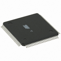
ATMEGA3250PV-10AU Atmel, ATMEGA3250PV-10AU Datasheet - Page 92

ATMEGA3250PV-10AU
Manufacturer Part Number
ATMEGA3250PV-10AU
Description
IC MCU AVR 32K FLASH 100-TQFP
Manufacturer
Atmel
Series
AVR® ATmegar
Datasheet
1.ATMEGA3250P-20AU.pdf
(364 pages)
Specifications of ATMEGA3250PV-10AU
Core Processor
AVR
Core Size
8-Bit
Speed
10MHz
Connectivity
SPI, UART/USART, USI
Peripherals
Brown-out Detect/Reset, POR, PWM, WDT
Number Of I /o
69
Program Memory Size
32KB (16K x 16)
Program Memory Type
FLASH
Eeprom Size
1K x 8
Ram Size
2K x 8
Voltage - Supply (vcc/vdd)
1.8 V ~ 5.5 V
Data Converters
A/D 8x10b
Oscillator Type
Internal
Operating Temperature
-40°C ~ 85°C
Package / Case
100-TQFP, 100-VQFP
Processor Series
ATMEGA32x
Core
AVR8
Data Bus Width
8 bit
Data Ram Size
2 KB
Interface Type
SPI, UART, USI
Maximum Clock Frequency
10 MHz
Number Of Programmable I/os
69
Number Of Timers
3
Maximum Operating Temperature
+ 85 C
Mounting Style
SMD/SMT
Minimum Operating Temperature
- 40 C
On-chip Adc
10 bit, 8 Channel
Data Rom Size
1 KB
Operating Supply Voltage
1.8 V to 5.5 V
Operating Temperature Range
- 40 C to + 85 C
A/d Bit Size
10 bit
A/d Channels Available
8
Height
1 mm
Length
14 mm
Supply Voltage (max)
5.5 V
Supply Voltage (min)
1.8 V
Width
14 mm
For Use With
ATSTK600-TQFP100 - STK600 SOCKET/ADAPTER 100-TQFP770-1007 - ISP 4PORT ATMEL AVR MCU SPI/JTAG770-1005 - ISP 4PORT FOR ATMEL AVR MCU JTAG770-1004 - ISP 4PORT FOR ATMEL AVR MCU SPIATAVRISP2 - PROGRAMMER AVR IN SYSTEMATSTK504 - STARTER KIT AVR EXP MOD 100P LCD
Lead Free Status / RoHS Status
Lead free / RoHS Compliant
Other names
ATMEGA3250PV-8AU
ATMEGA3250PV-8AU
ATMEGA3250PV-8AU
Available stocks
Company
Part Number
Manufacturer
Quantity
Price
- Current page: 92 of 364
- Download datasheet (6Mb)
14.5
Output Compare Unit
The 8-bit comparator continuously compares TCNT0 with the Output Compare Register
(OCR0A). Whenever TCNT0 equals OCR0A, the comparator signals a match. A match will set
the Output Compare Flag (OCF0A) at the next timer clock cycle. If enabled (OCIE0A = 1 and
Global Interrupt Flag in SREG is set), the Output Compare Flag generates an Output Compare
interrupt. The OCF0A Flag is automatically cleared when the interrupt is executed. Alternatively,
the OCF0A Flag can be cleared by software by writing a logical one to its I/O bit location. The
Waveform Generator uses the match signal to generate an output according to operating mode
set by the WGM01:0 bits and Compare Output mode (COM0A1:0) bits. The max and bottom sig-
nals are used by the Waveform Generator for handling the special cases of the extreme values
in some modes of operation
(See Section “14.7” on page
94.).
Figure 14-3
shows a block diagram of the Output Compare unit.
Figure 14-3. Output Compare Unit, Block Diagram
DATA BUS
OCRnx
TCNTn
=
(8-bit Comparator )
OCFnx (Int.Req.)
top
bottom
Waveform Generator
OCnx
FOCn
WGMn1:0
COMnX1:0
The OCR0A Register is double buffered when using any of the Pulse Width Modulation (PWM)
modes. For the normal and Clear Timer on Compare (CTC) modes of operation, the double buff-
ering is disabled. The double buffering synchronizes the update of the OCR0 Compare Register
to either top or bottom of the counting sequence. The synchronization prevents the occurrence
of odd-length, non-symmetrical PWM pulses, thereby making the output glitch-free.
The OCR0A Register access may seem complex, but this is not case. When the double buffer-
ing is enabled, the CPU has access to the OCR0A Buffer Register, and if double buffering is
disabled the CPU will access the OCR0A directly.
ATmega325P/3250P
92
8023F–AVR–07/09
Related parts for ATMEGA3250PV-10AU
Image
Part Number
Description
Manufacturer
Datasheet
Request
R

Part Number:
Description:
Manufacturer:
Atmel Corporation
Datasheet:

Part Number:
Description:
IC AVR MCU 32K 16MHZ 100TQFP
Manufacturer:
Atmel
Datasheet:

Part Number:
Description:
IC AVR MCU 32K 16MHZ 100TQFP
Manufacturer:
Atmel
Datasheet:

Part Number:
Description:
MCU AVR 32K FLASH 16MHZ 100TQFP
Manufacturer:
Atmel
Datasheet:

Part Number:
Description:
Atmega3250 8-bit Microcontroller With In-system Programmable Flash
Manufacturer:
ATMEL Corporation

Part Number:
Description:
Manufacturer:
Atmel Corporation
Datasheet:

Part Number:
Description:
IC AVR MCU 32K 16MHZ 64-QFN
Manufacturer:
Atmel
Datasheet:

Part Number:
Description:
IC AVR MCU 32K 16MHZ 64TQFP
Manufacturer:
Atmel
Datasheet:

Part Number:
Description:
IC AVR MCU 32K 16MHZ 64TQFP
Manufacturer:
Atmel
Datasheet:

Part Number:
Description:
IC AVR MCU 32K 16MHZ 64-QFN
Manufacturer:
Atmel
Datasheet:

Part Number:
Description:
8-bit Microcontroller with In-System Programmable Flash
Manufacturer:
ATMEL [ATMEL Corporation]
Datasheet:

Part Number:
Description:
MCU AVR 32K FLASH 16MHZ 64TQFP
Manufacturer:
Atmel
Datasheet:

Part Number:
Description:
MCU AVR 32K FLASH 16MHZ 64QFN
Manufacturer:
Atmel
Datasheet:


