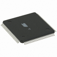
ATMEGA3250PV-10AU Atmel, ATMEGA3250PV-10AU Datasheet - Page 203

ATMEGA3250PV-10AU
Manufacturer Part Number
ATMEGA3250PV-10AU
Description
IC MCU AVR 32K FLASH 100-TQFP
Manufacturer
Atmel
Series
AVR® ATmegar
Datasheet
1.ATMEGA3250P-20AU.pdf
(364 pages)
Specifications of ATMEGA3250PV-10AU
Core Processor
AVR
Core Size
8-Bit
Speed
10MHz
Connectivity
SPI, UART/USART, USI
Peripherals
Brown-out Detect/Reset, POR, PWM, WDT
Number Of I /o
69
Program Memory Size
32KB (16K x 16)
Program Memory Type
FLASH
Eeprom Size
1K x 8
Ram Size
2K x 8
Voltage - Supply (vcc/vdd)
1.8 V ~ 5.5 V
Data Converters
A/D 8x10b
Oscillator Type
Internal
Operating Temperature
-40°C ~ 85°C
Package / Case
100-TQFP, 100-VQFP
Processor Series
ATMEGA32x
Core
AVR8
Data Bus Width
8 bit
Data Ram Size
2 KB
Interface Type
SPI, UART, USI
Maximum Clock Frequency
10 MHz
Number Of Programmable I/os
69
Number Of Timers
3
Maximum Operating Temperature
+ 85 C
Mounting Style
SMD/SMT
Minimum Operating Temperature
- 40 C
On-chip Adc
10 bit, 8 Channel
Data Rom Size
1 KB
Operating Supply Voltage
1.8 V to 5.5 V
Operating Temperature Range
- 40 C to + 85 C
A/d Bit Size
10 bit
A/d Channels Available
8
Height
1 mm
Length
14 mm
Supply Voltage (max)
5.5 V
Supply Voltage (min)
1.8 V
Width
14 mm
For Use With
ATSTK600-TQFP100 - STK600 SOCKET/ADAPTER 100-TQFP770-1007 - ISP 4PORT ATMEL AVR MCU SPI/JTAG770-1005 - ISP 4PORT FOR ATMEL AVR MCU JTAG770-1004 - ISP 4PORT FOR ATMEL AVR MCU SPIATAVRISP2 - PROGRAMMER AVR IN SYSTEMATSTK504 - STARTER KIT AVR EXP MOD 100P LCD
Lead Free Status / RoHS Status
Lead free / RoHS Compliant
Other names
ATMEGA3250PV-8AU
ATMEGA3250PV-8AU
ATMEGA3250PV-8AU
Available stocks
Company
Part Number
Manufacturer
Quantity
Price
- Current page: 203 of 364
- Download datasheet (6Mb)
20. Analog Comparator
20.1
20.2
8023F–AVR–07/09
Overview
Analog Comparator Multiplexed Input
The Analog Comparator compares the input values on the positive pin AIN0 and negative pin
AIN1. When the voltage on the positive pin AIN0 is higher than the voltage on the negative pin
AIN1, the Analog Comparator output, ACO, is set. The comparator’s output can be set to trigger
the Timer/Counter1 Input Capture function. In addition, the comparator can trigger a separate
interrupt, exclusive to the Analog Comparator. The user can select Interrupt triggering on com-
parator output rise, fall or toggle. A block diagram of the comparator and its surrounding logic is
shown in
The PRADC, in
the ADC input MUX.
Figure 20-1. Analog Comparator Block Diagram
Note:
It is possible to select any of the ADC7:0 pins to replace the negative input to the Analog Com-
parator. The ADC multiplexer is used to select this input, and consequently, the ADC must be
switched off to utilize this feature. If the Analog Comparator Multiplexer Enable bit (ACME in
ADCSRB) is set and the ADC is switched off (ADEN in ADCSRA is zero), MUX2:0 in ADMUX
select the input pin to replace the negative input to the Analog Comparator, as shown in
20-1. If ACME is cleared or ADEN is set, AIN1 is applied to the negative input to the Analog
Comparator.
Table 20-1.
ACME
0
1
1
ADC MULTIPLEXER
1. See
2. Refer to
Figure
REFERENCE
ACME
ADEN
BANDGAP
OUTPUT
page 75
Analog Comparator Multiplexed Input
Table 20-1 on page
(1)
”PRR – Power Reduction Register” on page 44
20-1.
ADEN
ACBG
x
1
0
Figure 1-1 on page
for Analog Comparator pin placement.
MUX2:0
000
xxx
xxx
203.
2,
Figure 1-2 on page
Analog Comparator Negative Input
AIN1
AIN1
ADC0
(2)
3and
ATmega325P/3250P
”Alternate Functions of Port E” on
must be written to zero to use
Table
203
Related parts for ATMEGA3250PV-10AU
Image
Part Number
Description
Manufacturer
Datasheet
Request
R

Part Number:
Description:
Manufacturer:
Atmel Corporation
Datasheet:

Part Number:
Description:
IC AVR MCU 32K 16MHZ 100TQFP
Manufacturer:
Atmel
Datasheet:

Part Number:
Description:
IC AVR MCU 32K 16MHZ 100TQFP
Manufacturer:
Atmel
Datasheet:

Part Number:
Description:
MCU AVR 32K FLASH 16MHZ 100TQFP
Manufacturer:
Atmel
Datasheet:

Part Number:
Description:
Atmega3250 8-bit Microcontroller With In-system Programmable Flash
Manufacturer:
ATMEL Corporation

Part Number:
Description:
Manufacturer:
Atmel Corporation
Datasheet:

Part Number:
Description:
IC AVR MCU 32K 16MHZ 64-QFN
Manufacturer:
Atmel
Datasheet:

Part Number:
Description:
IC AVR MCU 32K 16MHZ 64TQFP
Manufacturer:
Atmel
Datasheet:

Part Number:
Description:
IC AVR MCU 32K 16MHZ 64TQFP
Manufacturer:
Atmel
Datasheet:

Part Number:
Description:
IC AVR MCU 32K 16MHZ 64-QFN
Manufacturer:
Atmel
Datasheet:

Part Number:
Description:
8-bit Microcontroller with In-System Programmable Flash
Manufacturer:
ATMEL [ATMEL Corporation]
Datasheet:

Part Number:
Description:
MCU AVR 32K FLASH 16MHZ 64TQFP
Manufacturer:
Atmel
Datasheet:

Part Number:
Description:
MCU AVR 32K FLASH 16MHZ 64QFN
Manufacturer:
Atmel
Datasheet:


