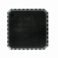
ATMEGA8L-8MU Atmel, ATMEGA8L-8MU Datasheet - Page 219

ATMEGA8L-8MU
Manufacturer Part Number
ATMEGA8L-8MU
Description
IC AVR MCU 8K 8MHZ 3V 32-QFN
Manufacturer
Atmel
Series
AVR® ATmegar
Specifications of ATMEGA8L-8MU
Core Processor
AVR
Core Size
8-Bit
Speed
8MHz
Connectivity
I²C, SPI, UART/USART
Peripherals
Brown-out Detect/Reset, POR, PWM, WDT
Number Of I /o
23
Program Memory Size
8KB (4K x 16)
Program Memory Type
FLASH
Eeprom Size
512 x 8
Ram Size
1K x 8
Voltage - Supply (vcc/vdd)
2.7 V ~ 5.5 V
Data Converters
A/D 8x10b
Oscillator Type
Internal
Operating Temperature
-40°C ~ 85°C
Package / Case
32-VQFN Exposed Pad, 32-HVQFN, 32-SQFN, 32-DHVQFN
Package
32MLF EP
Device Core
AVR
Family Name
ATmega
Maximum Speed
8 MHz
Operating Supply Voltage
3.3|5 V
Data Bus Width
8 Bit
Number Of Programmable I/os
23
Interface Type
SPI/TWI/USART
On-chip Adc
8-chx10-bit
Number Of Timers
3
Controller Family/series
AVR MEGA
No. Of I/o's
23
Eeprom Memory Size
512Byte
Ram Memory Size
1KB
Cpu Speed
8MHz
Rohs Compliant
Yes
For Use With
ATSTK600-TQFP32 - STK600 SOCKET/ADAPTER 32-TQFPATSTK600-DIP40 - STK600 SOCKET/ADAPTER 40-PDIP770-1007 - ISP 4PORT ATMEL AVR MCU SPI/JTAGATAVRISP2 - PROGRAMMER AVR IN SYSTEMATSTK500 - PROGRAMMER AVR STARTER KIT
Lead Free Status / RoHS Status
Lead free / RoHS Compliant
Available stocks
Company
Part Number
Manufacturer
Quantity
Price
Part Number:
ATMEGA8L-8MU
Manufacturer:
AT
Quantity:
20 000
- Current page: 219 of 302
- Download datasheet (6Mb)
Parallel
Programming
Parameters, Pin
Mapping, and
Commands
Signal Names
2486Z–AVR–02/11
This section describes how to parallel program and verify Flash Program memory, EEPROM
Data memory, Memory Lock Bits, and Fuse Bits in the ATmega8. Pulses are assumed to be at
least 250ns unless otherwise noted.
In this section, some pins of the ATmega8 are referenced by signal names describing their func-
tionality during parallel programming, see
following table are referenced by pin names.
The XA1/XA0 pins determine the action executed when the XTAL1 pin is given a positive pulse.
The bit coding is shown in
When pulsing WR or OE, the command loaded determines the action executed. The different
Commands are shown in
Figure 104. Parallel Programming
Table 91. Pin Name Mapping
Signal Name in
Programming Mode
RDY/BSY
OE
WR
BS1
XA0
XA1
Table 94 on page
Table 93 on page
Pin Name
RDY/BSY
PAGEL
+12 V
PD1
PD2
PD3
PD4
PD5
PD6
BS1
XA0
XA1
BS2
WR
OE
PD1
PD2
PD3
PD4
PD5
PD6
RESET
XTAL1
GND
PD7
PC2
I/O
O
I
I
I
I
I
Figure 104
220.
220.
PC[1:0]:PB[5:0]
Function
0: Device is busy programming, 1: Device
is ready for new command
Output Enable (Active low)
Write Pulse (Active low)
Byte Select 1 (“0” selects Low byte, “1”
selects High byte)
XTAL Action Bit 0
XTAL Action Bit 1
AVCC
VCC
and
Table
+5V
+5V
DATA
91. Pins not described in the
ATmega8(L)
219
Related parts for ATMEGA8L-8MU
Image
Part Number
Description
Manufacturer
Datasheet
Request
R

Part Number:
Description:
8-bit AVR with 8K Bytes In-System Programmable Flash
Manufacturer:
ATMEL [ATMEL Corporation]
Datasheet:

Part Number:
Description:
IC AVR MCU 8K 8MHZ 3V 28DIP
Manufacturer:
Atmel
Datasheet:

Part Number:
Description:
IC AVR MCU 8K LV 8MHZ COM 32TQFP
Manufacturer:
Atmel
Datasheet:

Part Number:
Description:
IC AVR MCU 8K LV 8MHZ IND 32TQFP
Manufacturer:
Atmel
Datasheet:

Part Number:
Description:
IC AVR MCU 8K LV 8MHZ COM 28-DIP
Manufacturer:
Atmel
Datasheet:

Part Number:
Description:
IC AVR MCU 8K LV 8MHZ IND 28-DIP
Manufacturer:
Atmel
Datasheet:

Part Number:
Description:
IC AVR MCU 8K LV 8MHZ COM 32-QFN
Manufacturer:
Atmel
Datasheet:

Part Number:
Description:
IC AVR MCU 8K LV 8MHZ IND 32-QFN
Manufacturer:
Atmel
Datasheet:

Part Number:
Description:
MCU AVR 8KB FLASH 8MHZ 32TQFP
Manufacturer:
Atmel
Datasheet:

Part Number:
Description:
MCU AVR 8KB FLASH 8MHZ 32QFN
Manufacturer:
Atmel
Datasheet:

Part Number:
Description:
IC MCU AVR 8K 5V 8MHZ 32-TQFP
Manufacturer:
Atmel
Datasheet:

Part Number:
Description:
IC MCU AVR 8K 5V 8MHZ 32-QFN
Manufacturer:
Atmel
Datasheet:

Part Number:
Description:
IC MCU AVR 8K 5V 8MHZ 28-DIP
Manufacturer:
Atmel
Datasheet:


