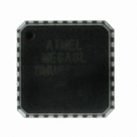
ATMEGA8L-8MU Atmel, ATMEGA8L-8MU Datasheet - Page 127

ATMEGA8L-8MU
Manufacturer Part Number
ATMEGA8L-8MU
Description
IC AVR MCU 8K 8MHZ 3V 32-QFN
Manufacturer
Atmel
Series
AVR® ATmegar
Specifications of ATMEGA8L-8MU
Core Processor
AVR
Core Size
8-Bit
Speed
8MHz
Connectivity
I²C, SPI, UART/USART
Peripherals
Brown-out Detect/Reset, POR, PWM, WDT
Number Of I /o
23
Program Memory Size
8KB (4K x 16)
Program Memory Type
FLASH
Eeprom Size
512 x 8
Ram Size
1K x 8
Voltage - Supply (vcc/vdd)
2.7 V ~ 5.5 V
Data Converters
A/D 8x10b
Oscillator Type
Internal
Operating Temperature
-40°C ~ 85°C
Package / Case
32-VQFN Exposed Pad, 32-HVQFN, 32-SQFN, 32-DHVQFN
Package
32MLF EP
Device Core
AVR
Family Name
ATmega
Maximum Speed
8 MHz
Operating Supply Voltage
3.3|5 V
Data Bus Width
8 Bit
Number Of Programmable I/os
23
Interface Type
SPI/TWI/USART
On-chip Adc
8-chx10-bit
Number Of Timers
3
Controller Family/series
AVR MEGA
No. Of I/o's
23
Eeprom Memory Size
512Byte
Ram Memory Size
1KB
Cpu Speed
8MHz
Rohs Compliant
Yes
For Use With
ATSTK600-TQFP32 - STK600 SOCKET/ADAPTER 32-TQFPATSTK600-DIP40 - STK600 SOCKET/ADAPTER 40-PDIP770-1007 - ISP 4PORT ATMEL AVR MCU SPI/JTAGATAVRISP2 - PROGRAMMER AVR IN SYSTEMATSTK500 - PROGRAMMER AVR STARTER KIT
Lead Free Status / RoHS Status
Lead free / RoHS Compliant
Available stocks
Company
Part Number
Manufacturer
Quantity
Price
Part Number:
ATMEGA8L-8MU
Manufacturer:
AT
Quantity:
20 000
- Current page: 127 of 302
- Download datasheet (6Mb)
SPI Data Register –
SPDR
Data Modes
2486Z–AVR–02/11
• Bit 7 – SPIF: SPI Interrupt Flag
When a serial transfer is complete, the SPIF Flag is set. An interrupt is generated if SPIE in
SPCR is set and global interrupts are enabled. If SS is an input and is driven low when the SPI is
in Master mode, this will also set the SPIF Flag. SPIF is cleared by hardware when executing the
corresponding interrupt Handling Vector. Alternatively, the SPIF bit is cleared by first reading the
SPI Status Register with SPIF set, then accessing the SPI Data Register (SPDR).
• Bit 6 – WCOL: Write COLlision Flag
The WCOL bit is set if the SPI Data Register (SPDR) is written during a data transfer. The
WCOL bit (and the SPIF bit) are cleared by first reading the SPI Status Register with WCOL set,
and then accessing the SPI Data Register.
• Bit 5..1 – Res: Reserved Bits
These bits are reserved bits in the ATmega8 and will always read as zero.
• Bit 0 – SPI2X: Double SPI Speed Bit
When this bit is written logic one the SPI speed (SCK Frequency) will be doubled when the SPI
is in Master mode (see
2 CPU clock periods. When the SPI is configured as Slave, the SPI is only guaranteed to work at
f
The SPI interface on the ATmega8 is also used for Program memory and EEPROM download-
ing or uploading. See
The SPI Data Register is a Read/Write Register used for data transfer between the Register File
and the SPI Shift Register. Writing to the register initiates data transmission. Reading the regis-
ter causes the Shift Register Receive buffer to be read.
There are four combinations of SCK phase and polarity with respect to serial data, which are
determined by control bits CPHA and CPOL. The SPI data transfer formats are shown in
59 on page 128
edges of the SCK signal, ensuring sufficient time for data signals to stabilize. This is clearly seen
by summarizing
Table 51. CPOL and CPHA Functionality
osc
Bit
Read/Write
Initial Value
/4 or lower.
CPOL = 0, CPHA = 0
CPOL = 0, CPHA = 1
CPOL = 1, CPHA = 0
CPOL = 1, CPHA = 1
MSB
R/W
X
7
and
Table 48 on page 126
Figure 60 on page
page 230
R/W
Table 50 on page
X
6
Sample (Falling)
Sample (Rising)
Leading Edge
Setup (Rising)
Setup (Falling)
R/W
for Serial Programming and verification.
5
X
and
R/W
128. Data bits are shifted out and latched in on opposite
4
X
126). This means that the minimum SCK period will be
Table 49 on page
R/W
X
3
Sample (Falling)
Sample (Rising)
Setup (Falling)
Trailing Edge
Setup (Rising)
R/W
X
2
126, as done below:
R/W
X
1
LSB
R/W
ATmega8(L)
0
X
SPI Mode
0
1
2
3
Undefined
SPDR
Figure
127
Related parts for ATMEGA8L-8MU
Image
Part Number
Description
Manufacturer
Datasheet
Request
R

Part Number:
Description:
8-bit AVR with 8K Bytes In-System Programmable Flash
Manufacturer:
ATMEL [ATMEL Corporation]
Datasheet:

Part Number:
Description:
IC AVR MCU 8K 8MHZ 3V 28DIP
Manufacturer:
Atmel
Datasheet:

Part Number:
Description:
IC AVR MCU 8K LV 8MHZ COM 32TQFP
Manufacturer:
Atmel
Datasheet:

Part Number:
Description:
IC AVR MCU 8K LV 8MHZ IND 32TQFP
Manufacturer:
Atmel
Datasheet:

Part Number:
Description:
IC AVR MCU 8K LV 8MHZ COM 28-DIP
Manufacturer:
Atmel
Datasheet:

Part Number:
Description:
IC AVR MCU 8K LV 8MHZ IND 28-DIP
Manufacturer:
Atmel
Datasheet:

Part Number:
Description:
IC AVR MCU 8K LV 8MHZ COM 32-QFN
Manufacturer:
Atmel
Datasheet:

Part Number:
Description:
IC AVR MCU 8K LV 8MHZ IND 32-QFN
Manufacturer:
Atmel
Datasheet:

Part Number:
Description:
MCU AVR 8KB FLASH 8MHZ 32TQFP
Manufacturer:
Atmel
Datasheet:

Part Number:
Description:
MCU AVR 8KB FLASH 8MHZ 32QFN
Manufacturer:
Atmel
Datasheet:

Part Number:
Description:
IC MCU AVR 8K 5V 8MHZ 32-TQFP
Manufacturer:
Atmel
Datasheet:

Part Number:
Description:
IC MCU AVR 8K 5V 8MHZ 32-QFN
Manufacturer:
Atmel
Datasheet:

Part Number:
Description:
IC MCU AVR 8K 5V 8MHZ 28-DIP
Manufacturer:
Atmel
Datasheet:


