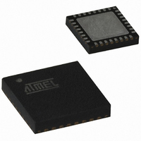
ATTINY28V-1MU Atmel, ATTINY28V-1MU Datasheet - Page 35

ATTINY28V-1MU
Manufacturer Part Number
ATTINY28V-1MU
Description
IC MCU AVR 2K 1.8V 1.2MHZ 32-QFN
Manufacturer
Atmel
Series
AVR® ATtinyr
Specifications of ATTINY28V-1MU
Core Processor
AVR
Core Size
8-Bit
Speed
1.2MHz
Peripherals
POR, WDT
Number Of I /o
11
Program Memory Size
2KB (1K x 16)
Program Memory Type
FLASH
Voltage - Supply (vcc/vdd)
1.8 V ~ 5.5 V
Oscillator Type
Internal
Operating Temperature
-40°C ~ 85°C
Package / Case
32-VQFN Exposed Pad, 32-HVQFN, 32-SQFN, 32-DHVQFN
Processor Series
ATTINY2x
Core
AVR8
Data Bus Width
8 bit
Data Ram Size
32 B
Maximum Clock Frequency
1.2 MHz
Number Of Programmable I/os
11
Number Of Timers
1
Operating Supply Voltage
1.8 V to 5.5 V
Maximum Operating Temperature
+ 85 C
Mounting Style
SMD/SMT
Minimum Operating Temperature
- 40 C
On-chip Adc
8 bit
For Use With
ATSTK600-DIP40 - STK600 SOCKET/ADAPTER 40-PDIPATSTK500 - PROGRAMMER AVR STARTER KIT
Lead Free Status / RoHS Status
Lead free / RoHS Compliant
Eeprom Size
-
Ram Size
-
Data Converters
-
Connectivity
-
Lead Free Status / Rohs Status
Details
Register Description
Timer/Counter0 Control
Register – TCCR0
1062F–AVR–07/06
The 8-bit Timer/Counter0 can select clock source from CK, prescaled CK or an external
pin. In addition, it can be stopped as described in the specification for the
Timer/Counter0 Control Register (TCCR0). The overflow status flag is found in the Inter-
rupt Flag Register (IFR). Control signals are found in the Timer/Counter0 Control
Register (TCCR0). The interrupt enable/disable setting for Timer/Counter0 is found in
the Interrupt Control Register (ICR).
When Timer/Counter0 is externally clocked, the external signal is synchronized with the
oscillator frequency of the CPU. To ensure proper sampling of the external clock, the
minimum time between two external clock transitions must be at least one internal CPU
clock period. The external clock signal is sampled on the rising edge of the internal CPU
clock.
The 8-bit Timer/Counter0 features both a high-resolution and a high-accuracy usage
with the lower prescaling opportunities. Similarly, the high prescaling opportunities make
the Timer/Counter0 useful for lower speed functions or exact timing functions with infre-
quent actions.
• Bit 7 – FOV0: Force Overflow
Writing a logical “1” to this bit forces a change on the overflow output pin PA2 according
to the values already set in OOM01 and OOM00. If the OOM01 and OOM00 bits are
written in the same cycle as FOV0, the new settings will not take effect until the next
overflow or forced overflow occurs. The Force Overflow bit can be used to change the
output pin without waiting for an overflow in the timer. The automatic action programmed
in OOM01 and OOM00 happens as if an overflow had occurred, but no interrupt is gen-
erated. The FOV0 bit will always read as zero, and writing a zero to this bit has no effect.
• Bits 6, 5 – Res: Reserved Bits
These bits are reserved bits in the ATtiny28 and always read as zero.
• Bits 4, 3 – OOM01, OOM00: Overflow Output Mode, Bits 1 and 0
The OOM01 and OOM00 control bits determine any output pin action following an over-
flow or a forced overflow in Timer/Counter0. Any output pin actions affect pin PA2. The
control configuration is shown in Table 13.
Table 13. Overflow Output Mode Select
Bit
$04
Read/Write
Initial Value
OOM01
0
0
1
1
FOV0
R/W
7
0
OOM00
0
1
0
1
R
6
–
0
Description
Timer/Counter0 disconnected from output pin PA2
Toggle the PA2 output line.
Clear the PA2 output line to zero.
Set the PA2 output line to one.
R
5
–
0
OOM01
R/W
4
0
OOM00
R/W
3
0
CS02
R/W
2
0
ATtiny28L/V
CS01
R/W
1
0
CS00
R/W
0
0
TCCR0
35


