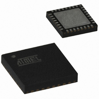
ATTINY28V-1MU Atmel, ATTINY28V-1MU Datasheet - Page 22

ATTINY28V-1MU
Manufacturer Part Number
ATTINY28V-1MU
Description
IC MCU AVR 2K 1.8V 1.2MHZ 32-QFN
Manufacturer
Atmel
Series
AVR® ATtinyr
Specifications of ATTINY28V-1MU
Core Processor
AVR
Core Size
8-Bit
Speed
1.2MHz
Peripherals
POR, WDT
Number Of I /o
11
Program Memory Size
2KB (1K x 16)
Program Memory Type
FLASH
Voltage - Supply (vcc/vdd)
1.8 V ~ 5.5 V
Oscillator Type
Internal
Operating Temperature
-40°C ~ 85°C
Package / Case
32-VQFN Exposed Pad, 32-HVQFN, 32-SQFN, 32-DHVQFN
Processor Series
ATTINY2x
Core
AVR8
Data Bus Width
8 bit
Data Ram Size
32 B
Maximum Clock Frequency
1.2 MHz
Number Of Programmable I/os
11
Number Of Timers
1
Operating Supply Voltage
1.8 V to 5.5 V
Maximum Operating Temperature
+ 85 C
Mounting Style
SMD/SMT
Minimum Operating Temperature
- 40 C
On-chip Adc
8 bit
For Use With
ATSTK600-DIP40 - STK600 SOCKET/ADAPTER 40-PDIPATSTK500 - PROGRAMMER AVR STARTER KIT
Lead Free Status / RoHS Status
Lead free / RoHS Compliant
Eeprom Size
-
Ram Size
-
Data Converters
-
Connectivity
-
Lead Free Status / Rohs Status
Details
Register Description
Interrupt Control Register –
ICR
22
ATtiny28L/V
• Bit 7 – INT1: External Interrupt Request 1 Enable
When the INT1 bit is set (one) and I-bit in the Status Register (SREG) is set (one), the
external pin interrupt 1 is enabled. The interrupt Sense Control1 bits 1/0 (ISC11 and
ISC10) define whether the external interrupt is activated on rising or falling edge, on pin
change or low level of the INT1 pin. The corresponding interrupt of External Interrupt
Request 1 is executed from program memory address $002. See also “External
Interrupt”.
• Bit 6 – INT0: External Interrupt Request 0 Enable
When the INT0 bit is set (one) and the I-bit in the Status Register (SREG) is set (one),
the external pin interrupt 0 is enabled. The interrupt Sense Control0 bits 1/0 (ISC01 and
ISC00) define whether the external interrupt is activated on rising or falling edge, on pin
change or low level of the INT0 pin. The corresponding interrupt of External Interrupt
Request 0 is executed from program memory address $001. See also “External
Interrupt”.
• Bit 5 – LLIE: Low-level Input Interrupt Enable
When the LLIE is set (one) and the I-bit in the status register (SREG) is set (one), the
interrupt on low-level input is activated. Any of the Port B pins pulled low will then cause
an interrupt. However, if any Port B pins are used for other special features, these pins
will not trigger the interrupt. The corresponding interrupt of Low-level Input Interrupt
Request is executed from program memory address $003. See also “Low-level Input
Interrupt”.
• Bit 4 – TOIE0: Timer/Counter0 Overflow Interrupt Enable
When the TOIE0 bit is set (one) and the I-bit in the Status Register is set (one), the
Timer/Counter0 Overflow Interrupt is enabled. The corresponding interrupt (at vector
$004) is executed if an overflow in Timer/Counter0 occurs, i.e., when the TOV0 bit is set
in the Interrupt Flag Register (IFR).
• Bits 3, 2 – ISC11, ISC10: Interrupt Sense Control 1 Bit 1 and Bit 0
The External Interrupt 1 is activated by the external pin INT1 if the SREG I-flag and the
corresponding interrupt enable are set. The level and edges on the external INT1 pin
that activate the interrupt are defined in Table 8.
Bit
$06
Read/Write
Initial Value
INT1
R/W
7
0
INT0
R/W
6
0
LLIE
R/W
5
0
TOIE0
R/W
4
0
ISC11
R/W
3
0
ISC10
R/W
2
0
ISC01
R/W
1
0
ISC00
R/W
1062F–AVR–07/06
0
0
ICR


