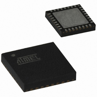
ATTINY28V-1MU Atmel, ATTINY28V-1MU Datasheet - Page 30

ATTINY28V-1MU
Manufacturer Part Number
ATTINY28V-1MU
Description
IC MCU AVR 2K 1.8V 1.2MHZ 32-QFN
Manufacturer
Atmel
Series
AVR® ATtinyr
Specifications of ATTINY28V-1MU
Core Processor
AVR
Core Size
8-Bit
Speed
1.2MHz
Peripherals
POR, WDT
Number Of I /o
11
Program Memory Size
2KB (1K x 16)
Program Memory Type
FLASH
Voltage - Supply (vcc/vdd)
1.8 V ~ 5.5 V
Oscillator Type
Internal
Operating Temperature
-40°C ~ 85°C
Package / Case
32-VQFN Exposed Pad, 32-HVQFN, 32-SQFN, 32-DHVQFN
Processor Series
ATTINY2x
Core
AVR8
Data Bus Width
8 bit
Data Ram Size
32 B
Maximum Clock Frequency
1.2 MHz
Number Of Programmable I/os
11
Number Of Timers
1
Operating Supply Voltage
1.8 V to 5.5 V
Maximum Operating Temperature
+ 85 C
Mounting Style
SMD/SMT
Minimum Operating Temperature
- 40 C
On-chip Adc
8 bit
For Use With
ATSTK600-DIP40 - STK600 SOCKET/ADAPTER 40-PDIPATSTK500 - PROGRAMMER AVR STARTER KIT
Lead Free Status / RoHS Status
Lead free / RoHS Compliant
Eeprom Size
-
Ram Size
-
Data Converters
-
Connectivity
-
Lead Free Status / Rohs Status
Details
Port D
Port D as General Digital I/O
30
ATtiny28L/V
Figure 26. PORT B Schematic Diagram (Pins PB7 - PB5)
Port D is an 8-bit bi-directional I/O port with internal pull-up resistors.
Three I/O memory address locations are allocated for Port D, one each for the Data
Register – PORTD, $12, Data Direction Register – DDRD, $11 and the Port D Input Pins
– PIND, $10. The Port D Input Pins address is read-only, while the Data Register and
the Data Direction Register are read/write.
The Port D output buffers can sink 10 mA. As inputs, Port D pins that are externally
pulled low will source current if the pull-up resistors are activated.
All eight pins in Port D have equal functionality when used as digital I/O pins.
PDn, general I/O pin: The DDDn bit in the DDRD register selects the direction of this pin.
If DDDn is set (one), PDn is configured as an output pin. If DDDn is cleared (zero), PDn
is configured as an input pin. If PDn is set (one) when configured as an input pin, the
MOS pull-up resistor is activated. To switch the pull-up resistor off, the PDn has to be
cleared (zero), or the pin has to be configured as an output pin. The port pins are tri-
stated when a reset condition becomes active, even if the clock is not running.
Table 12. DDDn Bits on Port D Pins
Note:
DDDn
0
0
1
1
PBn
n: 7,6,...,0, pin number
MOS
PULL-
UP
PORTDn
RP:
n:
0
1
0
1
READ PORT B PIN
5 - 7
Output
Output
Input
Input
I/O
Pull-up
Yes
NO
No
No
Comment
Tri-state (high-Z)
PDn will source current if ext. pulled low
Push-pull Zero Output
Push-pull One Output
RP
TO LOW-LEVEL DETECTOR
PULL-UP PORT B
1062F–AVR–07/06


