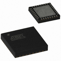
ATTINY28V-1MU Atmel, ATTINY28V-1MU Datasheet - Page 13

ATTINY28V-1MU
Manufacturer Part Number
ATTINY28V-1MU
Description
IC MCU AVR 2K 1.8V 1.2MHZ 32-QFN
Manufacturer
Atmel
Series
AVR® ATtinyr
Specifications of ATTINY28V-1MU
Core Processor
AVR
Core Size
8-Bit
Speed
1.2MHz
Peripherals
POR, WDT
Number Of I /o
11
Program Memory Size
2KB (1K x 16)
Program Memory Type
FLASH
Voltage - Supply (vcc/vdd)
1.8 V ~ 5.5 V
Oscillator Type
Internal
Operating Temperature
-40°C ~ 85°C
Package / Case
32-VQFN Exposed Pad, 32-HVQFN, 32-SQFN, 32-DHVQFN
Processor Series
ATTINY2x
Core
AVR8
Data Bus Width
8 bit
Data Ram Size
32 B
Maximum Clock Frequency
1.2 MHz
Number Of Programmable I/os
11
Number Of Timers
1
Operating Supply Voltage
1.8 V to 5.5 V
Maximum Operating Temperature
+ 85 C
Mounting Style
SMD/SMT
Minimum Operating Temperature
- 40 C
On-chip Adc
8 bit
For Use With
ATSTK600-DIP40 - STK600 SOCKET/ADAPTER 40-PDIPATSTK500 - PROGRAMMER AVR STARTER KIT
Lead Free Status / RoHS Status
Lead free / RoHS Compliant
Eeprom Size
-
Ram Size
-
Data Converters
-
Connectivity
-
Lead Free Status / Rohs Status
Details
Memory Access and
Instruction Execution
Timing
Flash Program Memory
1062F–AVR–07/06
Constant byte address is specified by the Z-register contents. The 15 MSBs select word
address (0 - 1K), and LSB selects low byte if cleared (LSB = 0) or high byte if set (LSB =
1).
This section describes the general access timing concepts for instruction execution and
internal memory access.
The AVR CPU is driven by the System Clock, directly generated from the external clock
crystal for the chip. No internal clock division is used.
Figure 14 shows the parallel instruction fetches and instruction executions enabled by
the Harvard architecture and the fast-access register file concept. This is the basic pipe-
lining concept to obtain up to 1 MIPS per MHz with the corresponding unique results for
functions per cost, functions per clocks and functions per power unit.
Figure 14. The Parallel Instruction Fetches and Instruction Executions
Figure 15 shows the internal timing concept for the register file. In a single clock cycle
an ALU operation using two register operands is executed, and the result is stored back
to the destination register.
Figure 15. Single Cycle ALU Operation
The ATtiny28 contains 2K bytes of on-chip Flash memory for program storage. Since all
instructions are single 16-bit words, the Flash is organized as 1K x 16 words. The Flash
memory has an endurance of at least 1,000 write/erase cycles.
The ATtiny28 program counter is 10 bits wide, thus addressing the 1K word Flash pro-
gram memory. See “Programming the Flash” on page 47 for a detailed description of
Flash data downloading.
2nd Instruction Execute
3rd Instruction Execute
1st Instruction Execute
Register Operands Fetch
ALU Operation Execute
2nd Instruction Fetch
3rd Instruction Fetch
4th Instruction Fetch
1st Instruction Fetch
Total Execution Time
System Clock Ø
Result Write Back
System Clock Ø
T1
T1
T2
T2
T3
ATtiny28L/V
T3
T4
T4
13


