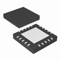
PIC18LF13K50-I/MQ Microchip Technology, PIC18LF13K50-I/MQ Datasheet - Page 228

PIC18LF13K50-I/MQ
Manufacturer Part Number
PIC18LF13K50-I/MQ
Description
IC PIC MCU FLASH 512KX8 20-QFN
Manufacturer
Microchip Technology
Series
PIC® XLP™ 18Fr
Datasheets
1.PIC18F13K50-ISS.pdf
(420 pages)
2.PIC18F13K50-ISS.pdf
(40 pages)
3.PIC18F13K50-ISS.pdf
(10 pages)
4.PIC18F13K50-ISS.pdf
(2 pages)
5.PIC18F14K50-IP.pdf
(422 pages)
Specifications of PIC18LF13K50-I/MQ
Program Memory Type
FLASH
Program Memory Size
8KB (4K x 16)
Package / Case
20-QFN
Core Processor
PIC
Core Size
8-Bit
Speed
48MHz
Connectivity
I²C, SPI, UART/USART, USB
Peripherals
Brown-out Detect/Reset, POR, PWM, WDT
Number Of I /o
14
Eeprom Size
256 x 8
Ram Size
512 x 8
Voltage - Supply (vcc/vdd)
1.8 V ~ 3.6 V
Data Converters
A/D 11x10b
Oscillator Type
Internal
Operating Temperature
-40°C ~ 85°C
Processor Series
PIC18LF
Core
PIC
Data Bus Width
8 bit
Data Ram Size
512 B
Interface Type
EUSART/I2C/MSSP/SPI/USB
Maximum Clock Frequency
48 MHz
Number Of Programmable I/os
15
Number Of Timers
4
Operating Supply Voltage
1.8 V to 3.6 V
Maximum Operating Temperature
+ 85 C
Mounting Style
SMD/SMT
3rd Party Development Tools
52715-96, 52716-328, 52717-734, 52712-325, EWPIC18
Development Tools By Supplier
PG164130, DV164035, DV244005, DV164005, DM164127, DV164126
Minimum Operating Temperature
- 40 C
On-chip Adc
11-ch x 10-bit
Controller Family/series
PIC18
No. Of I/o's
15
Eeprom Memory Size
256Byte
Ram Memory Size
512Byte
Cpu Speed
48MHz
No. Of Timers
4
Lead Free Status / RoHS Status
Lead free / RoHS Compliant
Lead Free Status / RoHS Status
Lead free / RoHS Compliant, Lead free / RoHS Compliant
Available stocks
Company
Part Number
Manufacturer
Quantity
Price
Company:
Part Number:
PIC18LF13K50-I/MQ
Manufacturer:
MICROCHIP
Quantity:
2 400
- PIC18F13K50-ISS PDF datasheet
- PIC18F13K50-ISS PDF datasheet #2
- PIC18F13K50-ISS PDF datasheet #3
- PIC18F13K50-ISS PDF datasheet #4
- PIC18F14K50-IP PDF datasheet #5
- Current page: 228 of 422
- Download datasheet (5Mb)
PIC18F/LF1XK50
18.2
Each
Configuration register: CM1CON0 for Comparator C1
and CM2CON0 for Comparator C2. In addition,
Comparator C2 has a second control register,
CM2CON1, for controlling the interaction with Timer1 and
simultaneous reading of both comparator outputs.
The CM1CON0 and CM2CON0 registers (see Registers
18-1 and 18-2, respectively) contain the control and
status bits for the following:
• Enable
• Input selection
• Reference selection
• Output selection
• Output polarity
• Speed selection
18.2.1
Setting the CxON bit of the CMxCON0 register enables
the comparator for operation. Clearing the CxON bit
disables the comparator resulting in minimum current
consumption.
18.2.2
The CxCH<1:0> bits of the CMxCON0 register direct
one of four analog input pins to the comparator
inverting input.
18.2.3
Setting the CxR bit of the CMxCON0 register directs an
internal voltage reference or an analog input pin to the
non-inverting
Section 21.0
information on the Internal Voltage Reference module.
18.2.4
The output of the comparator can be monitored by
reading either the CxOUT bit of the CMxCON0 register
or the MCxOUT bit of the CM2CON1 register. In order
to make the output available for an external connection,
the following conditions must be true:
• CxOE bit of the CMxCON0 register must be set
• Corresponding TRIS bit must be cleared
• CxON bit of the CMxCON0 register must be set
Both comparators share the same output pin
(C12OUT). Priority is determined by the states of the
C1OE and C2OE bits.
DS41350D-page 228
Note:
comparator
Comparator Control
COMPARATOR ENABLE
COMPARATOR INPUT SELECTION
To use CxIN+ and C12INx- pins as analog
inputs, the appropriate bits must be set in
the ANSEL register and the corresponding
TRIS bits must also be set to disable the
output drivers.
COMPARATOR REFERENCE
SELECTION
COMPARATOR OUTPUT
SELECTION
“V
input
OLTAGE
has
of
a
R
the
EFERENCES
separate
comparator.
” for
control
more
See
and
Preliminary
TABLE 18-1:
18.2.5
Inverting the output of the comparator is functionally
equivalent to swapping the comparator inputs. The
polarity of the comparator output can be inverted by
setting the CxPOL bit of the CMxCON0 register.
Clearing the CxPOL bit results in a non-inverted output.
Table 18-2 shows the output state versus input
conditions, including polarity control.
TABLE 18-2:
18.2.6
The trade-off between speed or power can be opti-
mized during program execution with the CxSP control
bit. The default state for this bit is ‘1’ which selects the
normal speed mode. Device power consumption can
be optimized at the cost of slower comparator propaga-
tion delay by clearing the CxSP bit to ‘0’.
18.3
The comparator output is indeterminate for a period of
time after the change of an input source or the selection
of a new reference voltage. This period is referred to as
the response time. The response time of the
comparator differs from the settling time of the voltage
reference. Therefore, both of these times must be
considered when determining the total response time
to a comparator input change. See the Comparator and
Voltage Reference Specifications in Section 27.0
“Electrical Specifications” for more details.
Input Condition
CxV
CxV
CxV
CxV
Note 1: The CxOE bit overrides the PORT data
C10E
IN
IN
IN
IN
0
0
1
1
- > CxV
- < CxV
- > CxV
- < CxV
2: The internal output of the comparator is
Comparator Response Time
COMPARATOR OUTPUT POLARITY
COMPARATOR SPEED SELECTION
latch. Setting the CxON has no impact on
the port override.
latched with each instruction cycle.
Unless otherwise specified, external
outputs are not latched.
IN
IN
IN
IN
+
+
+
+
COMPARATOR OUTPUT
PRIORITY
COMPARATOR OUTPUT
STATE VS. INPUT
CONDITIONS
C2OE
0
1
0
1
CxPOL
2010 Microchip Technology Inc.
0
0
1
1
C12OUT
C2OUT
C1OUT
C2OUT
CxOUT
I/O
0
1
1
0
Related parts for PIC18LF13K50-I/MQ
Image
Part Number
Description
Manufacturer
Datasheet
Request
R

Part Number:
Description:
Manufacturer:
Microchip Technology Inc.
Datasheet:

Part Number:
Description:
Manufacturer:
Microchip Technology Inc.
Datasheet:

Part Number:
Description:
Manufacturer:
Microchip Technology Inc.
Datasheet:

Part Number:
Description:
Manufacturer:
Microchip Technology Inc.
Datasheet:

Part Number:
Description:
Manufacturer:
Microchip Technology Inc.
Datasheet:

Part Number:
Description:
Manufacturer:
Microchip Technology Inc.
Datasheet:

Part Number:
Description:
Manufacturer:
Microchip Technology Inc.
Datasheet:

Part Number:
Description:
Manufacturer:
Microchip Technology Inc.
Datasheet:


