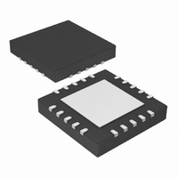
PIC18LF13K50-I/MQ Microchip Technology, PIC18LF13K50-I/MQ Datasheet - Page 211

PIC18LF13K50-I/MQ
Manufacturer Part Number
PIC18LF13K50-I/MQ
Description
IC PIC MCU FLASH 512KX8 20-QFN
Manufacturer
Microchip Technology
Series
PIC® XLP™ 18Fr
Datasheets
1.PIC18F13K50-ISS.pdf
(420 pages)
2.PIC18F13K50-ISS.pdf
(40 pages)
3.PIC18F13K50-ISS.pdf
(10 pages)
4.PIC18F13K50-ISS.pdf
(2 pages)
5.PIC18F14K50-IP.pdf
(422 pages)
Specifications of PIC18LF13K50-I/MQ
Program Memory Type
FLASH
Program Memory Size
8KB (4K x 16)
Package / Case
20-QFN
Core Processor
PIC
Core Size
8-Bit
Speed
48MHz
Connectivity
I²C, SPI, UART/USART, USB
Peripherals
Brown-out Detect/Reset, POR, PWM, WDT
Number Of I /o
14
Eeprom Size
256 x 8
Ram Size
512 x 8
Voltage - Supply (vcc/vdd)
1.8 V ~ 3.6 V
Data Converters
A/D 11x10b
Oscillator Type
Internal
Operating Temperature
-40°C ~ 85°C
Processor Series
PIC18LF
Core
PIC
Data Bus Width
8 bit
Data Ram Size
512 B
Interface Type
EUSART/I2C/MSSP/SPI/USB
Maximum Clock Frequency
48 MHz
Number Of Programmable I/os
15
Number Of Timers
4
Operating Supply Voltage
1.8 V to 3.6 V
Maximum Operating Temperature
+ 85 C
Mounting Style
SMD/SMT
3rd Party Development Tools
52715-96, 52716-328, 52717-734, 52712-325, EWPIC18
Development Tools By Supplier
PG164130, DV164035, DV244005, DV164005, DM164127, DV164126
Minimum Operating Temperature
- 40 C
On-chip Adc
11-ch x 10-bit
Controller Family/series
PIC18
No. Of I/o's
15
Eeprom Memory Size
256Byte
Ram Memory Size
512Byte
Cpu Speed
48MHz
No. Of Timers
4
Lead Free Status / RoHS Status
Lead free / RoHS Compliant
Lead Free Status / RoHS Status
Lead free / RoHS Compliant, Lead free / RoHS Compliant
Available stocks
Company
Part Number
Manufacturer
Quantity
Price
Company:
Part Number:
PIC18LF13K50-I/MQ
Manufacturer:
MICROCHIP
Quantity:
2 400
- PIC18F13K50-ISS PDF datasheet
- PIC18F13K50-ISS PDF datasheet #2
- PIC18F13K50-ISS PDF datasheet #3
- PIC18F13K50-ISS PDF datasheet #4
- PIC18F14K50-IP PDF datasheet #5
- Current page: 211 of 422
- Download datasheet (5Mb)
17.0
The
conversion of an analog input signal to a 10-bit binary
representation of that signal. This device uses analog
inputs, which are multiplexed into a single sample and
hold circuit. The output of the sample and hold is
connected to the input of the converter. The converter
generates a 10-bit binary result via successive
approximation and stores the conversion result into the
ADC result registers (ADRESL and ADRESH).
The ADC voltage reference is software selectable to
either V
pins.
The ADC can generate an interrupt upon completion of
a conversion. This interrupt can be used to wake-up the
device from Sleep.
Figure 17-1 shows the block diagram of the ADC.
FIGURE 17-1:
2010 Microchip Technology Inc.
Analog-to-Digital
DD
ANALOG-TO-DIGITAL
CONVERTER (ADC) MODULE
, or a voltage applied to the external reference
ADC BLOCK DIAGRAM
AN10
AN11
AN3
AN4
AN5
AN6
AN7
AN8
AN9
Unused
Unused
Unused
Unused
Unused
Converter
DAC
FVR
CHS<3:0>
V
REF
V
(ADC)
-
REF
FVR
AV
+
0000
0001
0010
0011
0100
0101
0110
0111
1000
1001
1010
1011
1100
1101
1110
1111
SS
AV
PVCFG[1:0] = 01
DD
NVCFG[1:0] = 00
NVCFG[1:0] = 01
allows
PVCFG[1:0] = 10
PVCFG[1:0] = 00
GO/DONE
Preliminary
ADON
V
SS
ADC
PIC18F/LF1XK50
ADFM
ADRESH
0 = Left Justify
1 = Right Justify
10
ADRESL
10
DS41350D-page 211
Related parts for PIC18LF13K50-I/MQ
Image
Part Number
Description
Manufacturer
Datasheet
Request
R

Part Number:
Description:
Manufacturer:
Microchip Technology Inc.
Datasheet:

Part Number:
Description:
Manufacturer:
Microchip Technology Inc.
Datasheet:

Part Number:
Description:
Manufacturer:
Microchip Technology Inc.
Datasheet:

Part Number:
Description:
Manufacturer:
Microchip Technology Inc.
Datasheet:

Part Number:
Description:
Manufacturer:
Microchip Technology Inc.
Datasheet:

Part Number:
Description:
Manufacturer:
Microchip Technology Inc.
Datasheet:

Part Number:
Description:
Manufacturer:
Microchip Technology Inc.
Datasheet:

Part Number:
Description:
Manufacturer:
Microchip Technology Inc.
Datasheet:


