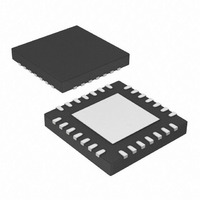
PIC18F23K20-I/MV Microchip Technology, PIC18F23K20-I/MV Datasheet - Page 267

PIC18F23K20-I/MV
Manufacturer Part Number
PIC18F23K20-I/MV
Description
IC MCU 8BIT 8KB FLASH 28UQFN
Manufacturer
Microchip Technology
Series
PIC® XLP™ 18Fr
Specifications of PIC18F23K20-I/MV
Program Memory Type
FLASH
Program Memory Size
8KB (4K x 16)
Package / Case
28-UFQFN Exposed Pad
Core Processor
PIC
Core Size
8-Bit
Speed
64MHz
Connectivity
I²C, SPI, UART/USART
Peripherals
Brown-out Detect/Reset, HLVD, POR, PWM, WDT
Number Of I /o
24
Eeprom Size
256 x 8
Ram Size
512 x 8
Voltage - Supply (vcc/vdd)
1.8 V ~ 3.6 V
Data Converters
A/D 11x10b
Oscillator Type
Internal
Operating Temperature
-40°C ~ 85°C
Processor Series
PIC18F
Core
PIC
Data Bus Width
16 bit
Data Ram Size
768 B
Interface Type
MSSP, I2C, SPI, USART
Maximum Clock Frequency
64 MHz
Number Of Programmable I/os
25
Number Of Timers
4
Operating Supply Voltage
1.8 V to 3.6 V
Maximum Operating Temperature
+ 125 C
Mounting Style
SMD/SMT
3rd Party Development Tools
52715-96, 52716-328, 52717-734, 52712-325, EWPIC18
Development Tools By Supplier
PG164130, DV164035, DV244005, DV164005
Minimum Operating Temperature
- 40 C
On-chip Adc
10 bit, 10 Channel
A/d Bit Size
10 bit
A/d Channels Available
10
Lead Free Status / RoHS Status
Lead free / RoHS Compliant
Lead Free Status / RoHS Status
Lead free / RoHS Compliant, Lead free / RoHS Compliant
Available stocks
Company
Part Number
Manufacturer
Quantity
Price
- Current page: 267 of 456
- Download datasheet (4Mb)
19.1.6
The ADC module allows for the ability to generate an
interrupt upon completion of an Analog-to-Digital
Conversion. The ADC interrupt flag is the ADIF bit in
the PIR1 register. The ADC interrupt enable is the ADIE
bit in the PIE1 register. The ADIF bit must be cleared by
software.
TABLE 19-1:
19.1.7
The 10-bit A/D conversion result can be supplied in two
formats, left justified or right justified. The ADFM bit of
the ADCON2 register controls the output format.
Figure 19-2 shows the two output formats.
FIGURE 19-2:
2010 Microchip Technology Inc.
Legend: Shaded cells are outside of recommended range.
Note 1:
ADC Clock Source
Note:
F
F
F
2:
3:
4:
(ADFM = 0)
(ADFM = 1)
F
F
F
OSC
OSC
OSC
OSC
OSC
OSC
F
ADC Clock Period (T
RC
The F
These values violate the minimum required T
For faster conversion times, the selection of another clock source is recommended.
When the device frequency is greater than 1 MHz, the F
conversion will be performed during Sleep.
INTERRUPTS
The ADIF bit is set at the completion of
every conversion, regardless of whether
or not the ADC interrupt is enabled.
RESULT FORMATTING
/16
/32
/64
/2
/4
/8
RC
ADC CLOCK PERIOD (T
source has a typical T
10-BIT A/D CONVERSION RESULT FORMAT
MSB
bit 7
bit 7
Unimplemented: Read as ‘0’
ADCS<2:0>
AD
000
100
001
101
010
110
x11
)
ADRESH
AD
10-bit A/D Result
time of 1.7 s.
AD
31.25 ns
) V
1-4 s
62.5 ns
400 ns
250 ns
500 ns
64 MHz
1.0 s
S
. DEVICE OPERATING FREQUENCIES
MSB
(1,4)
AD
(2)
(2)
(2)
(2)
(2)
time.
bit 0
bit 0
This interrupt can be generated while the device is
operating or while in Sleep. If the device is in Sleep, the
interrupt will wake-up the device. Upon waking from
Sleep, the next instruction following the SLEEP
instruction is always executed. If the user is attempting
to wake-up from Sleep and resume in-line code
execution, the global interrupt must be disabled. If the
global interrupt is enabled, execution will switch to the
Interrupt Service Routine. Please see Section 19.1.6
“Interrupts” for more information.
PIC18F2XK20/4XK20
1-4 s
RC
125 ns
250 ns
500 ns
Device Frequency (F
4.0 s
16 MHz
1.0 s
2.0 s
clock source is only recommended if the
bit 7
bit 7
(1,4)
(3)
(2)
(2)
(2)
10-bit A/D Result
LSB
Unimplemented: Read as ‘0’
1-4 s
16.0 s
500 ns
4.0 s
8.0 s
4 MHz
1.0 s
2.0 s
ADRESL
OSC
(1,4)
(3)
(3)
(2)
(3)
)
DS41303G-page 267
1-4 s
16.0 s
32.0 s
64.0 s
4.0 s
8.0 s
1 MHz
2.0 s
bit 0
LSB
bit 0
(1,4)
(3)
(3)
(3)
(3)
(3)
Related parts for PIC18F23K20-I/MV
Image
Part Number
Description
Manufacturer
Datasheet
Request
R

Part Number:
Description:
Manufacturer:
Microchip Technology Inc.
Datasheet:

Part Number:
Description:
Manufacturer:
Microchip Technology Inc.
Datasheet:

Part Number:
Description:
Manufacturer:
Microchip Technology Inc.
Datasheet:

Part Number:
Description:
Manufacturer:
Microchip Technology Inc.
Datasheet:

Part Number:
Description:
Manufacturer:
Microchip Technology Inc.
Datasheet:

Part Number:
Description:
Manufacturer:
Microchip Technology Inc.
Datasheet:

Part Number:
Description:
Manufacturer:
Microchip Technology Inc.
Datasheet:

Part Number:
Description:
Manufacturer:
Microchip Technology Inc.
Datasheet:


