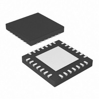
PIC18F23K20-I/MV Microchip Technology, PIC18F23K20-I/MV Datasheet - Page 149

PIC18F23K20-I/MV
Manufacturer Part Number
PIC18F23K20-I/MV
Description
IC MCU 8BIT 8KB FLASH 28UQFN
Manufacturer
Microchip Technology
Series
PIC® XLP™ 18Fr
Specifications of PIC18F23K20-I/MV
Program Memory Type
FLASH
Program Memory Size
8KB (4K x 16)
Package / Case
28-UFQFN Exposed Pad
Core Processor
PIC
Core Size
8-Bit
Speed
64MHz
Connectivity
I²C, SPI, UART/USART
Peripherals
Brown-out Detect/Reset, HLVD, POR, PWM, WDT
Number Of I /o
24
Eeprom Size
256 x 8
Ram Size
512 x 8
Voltage - Supply (vcc/vdd)
1.8 V ~ 3.6 V
Data Converters
A/D 11x10b
Oscillator Type
Internal
Operating Temperature
-40°C ~ 85°C
Processor Series
PIC18F
Core
PIC
Data Bus Width
16 bit
Data Ram Size
768 B
Interface Type
MSSP, I2C, SPI, USART
Maximum Clock Frequency
64 MHz
Number Of Programmable I/os
25
Number Of Timers
4
Operating Supply Voltage
1.8 V to 3.6 V
Maximum Operating Temperature
+ 125 C
Mounting Style
SMD/SMT
3rd Party Development Tools
52715-96, 52716-328, 52717-734, 52712-325, EWPIC18
Development Tools By Supplier
PG164130, DV164035, DV244005, DV164005
Minimum Operating Temperature
- 40 C
On-chip Adc
10 bit, 10 Channel
A/d Bit Size
10 bit
A/d Channels Available
10
Lead Free Status / RoHS Status
Lead free / RoHS Compliant
Lead Free Status / RoHS Status
Lead free / RoHS Compliant, Lead free / RoHS Compliant
Available stocks
Company
Part Number
Manufacturer
Quantity
Price
- Current page: 149 of 456
- Download datasheet (4Mb)
11.4
The PWM mode generates a Pulse-Width Modulated
signal on the CCP2 pin for the CCP module and the
P1A through P1D pins for the ECCP module. Hereafter
the modulated output pin will be referred to as the CCPx
pin. The duty cycle, period and resolution are
determined by the following registers:
• PR2
• T2CON
• CCPR
• CCPxCON
In Pulse-Width Modulation (PWM) mode, the CCP
module produces up to a 10-bit resolution PWM output
on the CCPx pin. Since the CCPx pin is multiplexed
with the PORT data latch, the TRIS for that pin must be
cleared to enable the CCPx pin output driver.
Figure 11.1.1 shows a simplified block diagram of
PWM operation.
Figure 11-4 shows a typical waveform of the PWM
signal.
For a step-by-step procedure on how to set up the CCP
module for PWM operation, see Section 11.4.7
“Setup for PWM Operation”.
FIGURE 11-3:
2010 Microchip Technology Inc.
Note 1:
Note:
CCPRxH
Duty Cycle Registers
Comparator
2:
x
CCPRxL
PWM Mode
PR2
L
TMR2
Comparator
Clearing the CCPxCON register will
relinquish CCPx control of the CCPx pin.
The 8-bit timer TMR2 register is concatenated
with the 2-bit internal system clock (F
2 bits of the prescaler, to create the 10-bit time
base.
In PWM mode, CCPRxH is a read-only register.
(2)
(Slave)
(1)
SIMPLIFIED PWM BLOCK
DIAGRAM
Clear Timer2,
toggle CCPx pin and
latch duty cycle
DCxB<1:0>
S
R
Q
TRIS
OSC
CCPx
), or
The PWM output (Figure 11-4) has a time base
(period) and a time that the output stays high (duty
cycle).
FIGURE 11-4:
PIC18F2XK20/4XK20
Pulse Width
TMR2 = 0
Period
CCP PWM OUTPUT
TMR2 = CCPRxL:DCxB<1:0>
TMR2 = PR2
DS41303G-page 149
Related parts for PIC18F23K20-I/MV
Image
Part Number
Description
Manufacturer
Datasheet
Request
R

Part Number:
Description:
Manufacturer:
Microchip Technology Inc.
Datasheet:

Part Number:
Description:
Manufacturer:
Microchip Technology Inc.
Datasheet:

Part Number:
Description:
Manufacturer:
Microchip Technology Inc.
Datasheet:

Part Number:
Description:
Manufacturer:
Microchip Technology Inc.
Datasheet:

Part Number:
Description:
Manufacturer:
Microchip Technology Inc.
Datasheet:

Part Number:
Description:
Manufacturer:
Microchip Technology Inc.
Datasheet:

Part Number:
Description:
Manufacturer:
Microchip Technology Inc.
Datasheet:

Part Number:
Description:
Manufacturer:
Microchip Technology Inc.
Datasheet:


