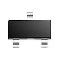
NUP1301,215 NXP Semiconductors, NUP1301,215 Datasheet - Page 8

NUP1301,215
Manufacturer Part Number
NUP1301,215
Description
IC DIODE ARRAY ESD SOT23-3
Manufacturer
NXP Semiconductors
Datasheet
1.NUP1301215.pdf
(13 pages)
Specifications of NUP1301,215
Package / Case
SOT-23-3, TO-236-3, Micro3™, SSD3, SST3
Power (watts)
220W
Polarization
2 Channel Array - Unidirectional
Voltage - Breakdown
100V
Voltage - Reverse Standoff (typ)
80V
Operating Voltage
1.25 V
Breakdown Voltage
100 V
Capacitance
0.6 pF
Termination Style
SMD/SMT
Power Dissipation Pd
250 mW
Operating Temperature Range
- 55 C to + 155 C
Lead Free Status / RoHS Status
Lead free / RoHS Compliant
Lead Free Status / RoHS Status
Lead free / RoHS Compliant, Lead free / RoHS Compliant
Other names
934063605215
NXP Semiconductors
8. Application information
9. Test information
NUP1301_1
Product data sheet
9.1 Quality information
Protection of a single (high-speed) data line in rail-to-rail configuration. The protected data
line is connected to pin 3. Pin 1 is connected to ground (GND) and pin 2 is connected to
the supply rail (supply voltage V
voltage drop of one diode, the transient is directed either to the supply rail or to GND.
The advantages of these solutions are: low line capacitance (0.6 pF typically), fast
response time, and low clamping voltage.
Circuit board layout and protection device placement:
Circuit board layout is critical for the suppression of ESD, Electrical Fast Transient (EFT)
and surge transients. The following guidelines are recommended:
This product has been qualified in accordance with the Automotive Electronics Council
(AEC) standard Q101 - Stress test qualification for discrete semiconductors , and is
suitable for use in automotive applications.
1. Place the NUP1301 as close to the input terminal or connector as possible.
2. The path length between the NUP1301 and the protected line should be minimized.
3. Keep parallel signal paths to a minimum.
4. Avoid running protected conductors in parallel with unprotected conductors.
5. Minimize all Printed-Circuit Board (PCB) conductive loops including power and
6. Minimize the length of the transient return path to ground.
7. Avoid using shared transient return paths to a common ground point.
8. Ground planes should be used whenever possible. For multilayer PCBs, use ground
Fig 8.
ground loops.
vias.
Typical application for the protection of one signal line
Rev. 01 — 11 May 2009
interface
Audio
CC
.) When the transient voltage exceeds the forward
V
CC
Ultra low capacitance ESD protection array
D1
NUP1301
V
CC
D2
NUP1301
006aab568
NUP1301
© NXP B.V. 2009. All rights reserved.
8 of 13


