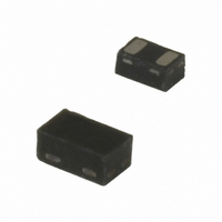
ESDALC6V1-1BM2 STMicroelectronics, ESDALC6V1-1BM2 Datasheet

ESDALC6V1-1BM2
Specifications of ESDALC6V1-1BM2
Available stocks
Related parts for ESDALC6V1-1BM2
ESDALC6V1-1BM2 Summary of contents
Page 1
... TM: Transil is a trademark of STMicroelectronics April 2008 2 Figure 1. Description The ESDALC6V1-1BM2 is a bidirectional single line TVS diode designed to protect the datalines or other I/O ports against ESD transients. The device is ideal for applications where both reduced line capacitance and board space saving are required. ...
Page 2
... Breakdown voltage BR V Clamping voltage CL I Leakage current @ Peak pulse current PP V Forward voltage drop F Order code ESDALC6V1-1BM2 2/ °C) amb Parameter = 25 °C) amb Parameter min. max. max 6.1 8.0 1 100 ESDALC6V1-1BM2 Value ± initial = T 140 j amb 9 125 - 150 260 - 125 typ. max /° ...
Page 3
... ESDALC6V1-1BM2 Figure 2. Relative variation of peak pulse power versus initial junction temperature P [T initial initial=25° 1.1 1.0 0.9 0.8 0.7 0.6 0.5 0.4 0.3 0.2 0.1 T (° Figure 4. Clamping voltage versus peak pulse current (typical values) I (A) PP 100.0 T initial=25° ...
Page 4
... Ordering information scheme Figure 10. Ordering information scheme ESD Array Low Capacitance Breakdown Voltage 6V1 = 6.1 Volts min Number of lines Directional B = Bi-directional Package M2 = SOD882 4/10 Figure 9. S21 attenuation measurement result dB 0. 10.00 - 20.00 - 30.00 F (Hz) - 40.00 100.0k 1.0M 10.0M ESDA LC 6V1 - ESDALC6V1-1BM2 100.0M 1.0G ...
Page 5
... ESDALC6V1-1BM2 3 Package information ● Epoxy meets UL94 order to meet environmental requirements, ST offers these devices in ECOPACK packages. These packages have a lead-free second level interconnect. The category of second level interconnect is marked on the inner box label, in compliance with JEDEC Standard JESD97. The maximum ratings related to soldering conditions are also marked on the inner box label ...
Page 6
... Package information Figure 13. Tape and reel specifications 0.20 ± 0.05 0.66 ± 0.05 (C-PAK) 0.55 ± 0.1 (3M) All dimensions in mm 6/10 Ø 1.55 ± 0.05 4.0 ± 0.1 2.0 ± 0.05 0.68 ± 0.05 2.0 ± 0.1 User direction of unreeling ESDALC6V1-1BM2 ...
Page 7
... ESDALC6V1-1BM2 4 Recommendation on PCB assembly 4.1 Stencil opening design 1. General recommendation on stencil opening design a) Stencil opening dimensions: L (Length), W (Width), T (Thickness). Figure 14. Stencil opening dimensions b) General design rule Stencil thickness ( 125 µm Aspect Ratio Aspect Area 2. Reference design a) Stencil opening thickness: 100 µm b) Stencil opening for leads: Opening to footprint ratio - between 60% and 65% ...
Page 8
... Note: Minimize air convection currents in the reflow oven to avoid component movement. 8/10 3°C/s max 3°C/s max 150 sec 90 to 150 sec ESDALC6V1-1BM2 2°C/s recommended 2°C/s recommended 6°C/s max 6°C/s max Time (min) Time (min) 10-30 sec 10-30 sec 90 sec max ...
Page 9
... ESDALC6V1-1BM2 5 Ordering information Table 4. Ordering information Order code ESDALC6V1-1BM2 1. The marking can be rotated by 90° to diferentiate assembly location 6 Revision history Table 5. Document revision history Date 11-Jan-2007 1-Apr-2007 Marking Package (1) P SOD882 Revision 1 Initial release. Reformatted to currrent standards. Added 2 Updated Figure 13.: Tape and reel ...
Page 10
... Australia - Belgium - Brazil - Canada - China - Czech Republic - Finland - France - Germany - Hong Kong - India - Israel - Italy - Japan - Malaysia - Malta - Morocco - Singapore - Spain - Sweden - Switzerland - United Kingdom - United States of America 10/10 Please Read Carefully: © 2008 STMicroelectronics - All rights reserved STMicroelectronics group of companies www.st.com ESDALC6V1-1BM2 ...


