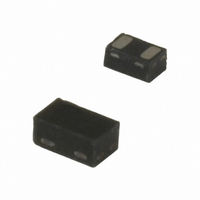
ESDALC6V1-1BT2 STMicroelectronics, ESDALC6V1-1BT2 Datasheet

ESDALC6V1-1BT2
Specifications of ESDALC6V1-1BT2
Available stocks
Related parts for ESDALC6V1-1BT2
ESDALC6V1-1BT2 Summary of contents
Page 1
... TM: Transil is a trademark of STMicroelectronics December 2010 2 Figure 1. Description The ESDALC6V1-1BT2 is a bidirectional single line TVS diode designed to protect the datalines or other I/O ports against ESD transients. The device is ideal for applications where both reduced line capacitance and board space saving are required. ...
Page 2
... Order code ESDALC6V1-1BT2 2/10 = 25° C) amb Parameter Parameter Breakdown voltage Stand-off voltage Clamping voltage Leakage current @ V RM Peak pulse current Forward voltage drop min. max. max 6.1 8.0 1 Doc ID 13909 Rev 2 ESDALC6V1-1BT2 Value ±30 T initial = T 100 j amb 9 125 - 150 260 - 125 ...
Page 3
... ESDALC6V1-1BT2 Figure 3. Relative variation of peak pulse power versus initial junction temperature P [T initial initial=25° 1.1 1.0 0.9 0.8 0.7 0.6 0.5 0.4 0.3 0.2 0.1 T (° Figure 5. Clamping voltage versus peak pulse current (typical values) I (A) PP 100.0 T initial=25° ...
Page 4
... Figure 11. Ordering information ESD array Low capacitance Breakdown voltage 6V1 = 6.1 volts min Number of lines Directional B = bidirectional Package T2 = thin SOD882 4/10 Figure 10. S21 attenuation measurement result 0.00 - 10.00 - 20.00 - 30.00 - 40.00 100.0k 1.0M ESDA LC 6V1 - Doc ID 13909 Rev 2 ESDALC6V1-1BT2 10.0M 100.0M 1.0G f/Hz ...
Page 5
... ESDALC6V1-1BT2 3 Package information ● Epoxy meets UL94, V0 ● Lead-free package In order to meet environmental requirements, ST offers these devices in different grades of ® ECOPACK packages, depending on their level of environmental compliance. ECOPACK specifications, grade definitions and product status are available at: www.st.com. ® ECOPACK trademark. Table 3. ...
Page 6
... Package information Figure 14. Tape and reel specifications 0.47 ± 0.05 All dimensions in mm 6/10 4.0 ± 0.1 2.0 ± 0.05 0.70 ± 0.05 User direction of unreeling Doc ID 13909 Rev 2 ESDALC6V1-1BT2 Ø 1.55 ± 0.05 2.0 ± 0.1 ...
Page 7
... ESDALC6V1-1BT2 4 Recommendation on PCB assembly 4.1 Stencil opening design 1. General recommendation on stencil opening design a) Stencil opening dimensions: L (Length), W (Width), T (Thickness). Figure 15. Stencil opening dimensions b) General design rule Stencil thickness ( 125 µm Aspect Ratio Aspect Area 2. Reference design a) Stencil opening thickness: 100 µm b) Stencil opening for leads: Opening to footprint ratio - between 60% and 65% ...
Page 8
... Note: Minimize air convection currents in the reflow oven to avoid component movement. 8/10 3°C/s max 3°C/s max 150 sec 90 to 150 sec Doc ID 13909 Rev 2 ESDALC6V1-1BT2 2°C/s recommended 2°C/s recommended 6°C/s max 6°C/s max Time (min) Time (min) 10-30 sec 10-30 sec ...
Page 9
... ESDALC6V1-1BT2 5 Ordering information Table 4. Ordering information Order code ESDALC6V1-1BT2 1. The marking can be rotated by 90° to differentiate assembly location 6 Revision history Table 5. Revision history Date 13-Sep-2007 02-Dec-2010 Marking Package Thin (1) L SOD882 Revision 1 Initial release. 2 Updated base quantity in Doc ID 13909 Rev 2 Ordering information ...
Page 10
... Australia - Belgium - Brazil - Canada - China - Czech Republic - Finland - France - Germany - Hong Kong - India - Israel - Italy - Japan - Malaysia - Malta - Morocco - Philippines - Singapore - Spain - Sweden - Switzerland - United Kingdom - United States of America 10/10 Please Read Carefully: © 2010 STMicroelectronics - All rights reserved STMicroelectronics group of companies www.st.com Doc ID 13909 Rev 2 ESDALC6V1-1BT2 ...


