MPC566EVB Freescale Semiconductor, MPC566EVB Datasheet - Page 54
MPC566EVB
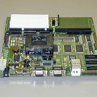
Manufacturer Part Number
MPC566EVB
Description
KIT EVALUATION FOR MPC565/566
Manufacturer
Freescale Semiconductor
Specifications of MPC566EVB
Processor To Be Evaluated
MPC56x
Data Bus Width
32 bit
Interface Type
RS-232, Ethernet
Lead Free Status / RoHS Status
Contains lead / RoHS non-compliant


Operational Procedure
Most commands can be recognized by using an abbreviated name. For instance, entering “h” is
the same as entering “help”. Thus, it is not necessary to type the entire command name.
The commands DI, GO, MD, STEP and TRACE are used repeatedly when debugging. dBUG
recognizes this and allows for repeated execution of these commands with minimal typing. After
a command is entered, simply press <RETURN> or <ENTER> to invoke the command again. The
command is executed as if no command line parameters were provided.
An additional function called the "System Call" allows the user program to utilize various routines
within dBUG. The System Call is discussed at the end of this chapter.
The operational mode of dBUG is demonstrated in Figure 3-1. After the system initialization, the
board waits for a command-line input from the user terminal. When a proper command is entered,
the operation continues in one of the two basic modes. If the command causes execution of the
user program, the dBUG firmware may or may not be re-entered, at the discretion of the user’s
program. For the alternate case, the command will be executed under control of the dBUG
firmware, and after command completion, the system returns to command entry mode.
During command execution, additional user input may be required depending on the command
function.
For commands that accept an optional <width> to modify the memory access size, the valid values
are:
When no <width> option is provided, the default width is .W, 32-bit.
The core MPC500 register set is maintained by dBUG. These are listed below:
All control registers on MPC500 core are not readable by the supervisor-programming model, and
thus not accessible via dBUG. User code may change these registers, but caution must be exercised
as changes may render dBUG inoperable.
A reference to “SP” (stack pointer) actually refers to general purpose address register one, “GPR1."
3.2 Operational Procedure
System power-up and initial operation are described in detail in Chapter 2. This information is
repeated here for convenience and to prevent possible damage.
3.2.1 System Power-up
3-2
•
•
•
•
•
•
•
•
•
B 8-bit (byte) access
H 16-bit (half-word) access
W 32-bit (word) access
GPR0-GPR31
IP (SRR0 is IP)
MSR (SRR1 is MSR)
CR, XER, LR, CTR, DSISR, DAR, DEC
Be sure the power supply is connected properly prior to power-up.
Make sure the terminal is connected to RS232 COM-1 connector.
Freescale Semiconductor, Inc.
For More Information On This Product,
MPC564EVB User’s Manual
Go to: www.freescale.com
Related parts for MPC566EVB
Image
Part Number
Description
Manufacturer
Datasheet
Request
R

Part Number:
Description:
Manufacturer:
Freescale Semiconductor, Inc
Datasheet:
Part Number:
Description:
Manufacturer:
Freescale Semiconductor, Inc
Datasheet:
Part Number:
Description:
Manufacturer:
Freescale Semiconductor, Inc
Datasheet:
Part Number:
Description:
Manufacturer:
Freescale Semiconductor, Inc
Datasheet:
Part Number:
Description:
Manufacturer:
Freescale Semiconductor, Inc
Datasheet:
Part Number:
Description:
Manufacturer:
Freescale Semiconductor, Inc
Datasheet:
Part Number:
Description:
Manufacturer:
Freescale Semiconductor, Inc
Datasheet:
Part Number:
Description:
Manufacturer:
Freescale Semiconductor, Inc
Datasheet:
Part Number:
Description:
Manufacturer:
Freescale Semiconductor, Inc
Datasheet:
Part Number:
Description:
Manufacturer:
Freescale Semiconductor, Inc
Datasheet:
Part Number:
Description:
Manufacturer:
Freescale Semiconductor, Inc
Datasheet:
Part Number:
Description:
Manufacturer:
Freescale Semiconductor, Inc
Datasheet:
Part Number:
Description:
Manufacturer:
Freescale Semiconductor, Inc
Datasheet:
Part Number:
Description:
Manufacturer:
Freescale Semiconductor, Inc
Datasheet:
Part Number:
Description:
Manufacturer:
Freescale Semiconductor, Inc
Datasheet: