MPC566EVB Freescale Semiconductor, MPC566EVB Datasheet - Page 30
MPC566EVB
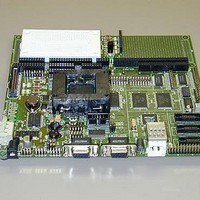
Manufacturer Part Number
MPC566EVB
Description
KIT EVALUATION FOR MPC565/566
Manufacturer
Freescale Semiconductor
Specifications of MPC566EVB
Processor To Be Evaluated
MPC56x
Data Bus Width
32 bit
Interface Type
RS-232, Ethernet
Lead Free Status / RoHS Status
Contains lead / RoHS non-compliant


Connectors and User Components
slowly compared to the MPC566 bus operation speeds so the LCD port provides a 16 bit wide
register port for access. The registered port allows writing the LCD module control signals and full
Read and Write capability for LCD module command and data bytes without the CPU waiting for
LCD access time. LCD Port access are performed as a 3 or 4 bus cycle transaction as follows:
Access cycle 1: Write LCD control bits RS, R/W, LCD data byte. LCD1 and 2 select bits = 0.
Access cycle 2: Write LCD control bits LCD1 select, LCD2 select active as required. RS, R/W,
LCD data byte values do not change but must be written again.
Access cycle 3 = READ: Read LCD Port if a Read access type, determined by R/W = 1 in first
access cycles.
Access cycle 3 = WRITE: Write LCD control bits LCD1 select, LCD2 select idle. RS, R/W, LCD
data byte do not change but must be written again. This terminates a Write access sequence.
Access cycle 4 = READ end: Write LCD control bits LCD1 select, LCD2 select idle, RS, R/W bits
do not change but must be written again. This terminates a Read access sequence.
Example source code for the LCD and Keypad drivers are provided on the Axiom MPC5xx support
CD. The LCD Port is assigned on chip select CS3 if enabled with MAP Switch position 6. Memory
map offset for the LCD Port = CS3 base + 0x0010.
LCD Display CONTRAST
The CONTRAST adjustment allows a contrast Vee voltage to be presented to the LCD_PORT of
–5V to +5V DC.
JP2 - LCD_PORT Power Polarity Select
JP2 determines the display power pin polarity on the LCD_PORT. Depending on the type and
location of the IDC connector on your display module, the power connections may need to be
reversed. Care should be used to verify proper connection and signal matching at the IDC Cable
Connector and LCD_PORT.
See the schematic to match this jumper setting to your LCD device connector. Contact
support@axman.com for assistance applying a LCD module.
1-20
Table 1-9. LCD PORT REGISTER Definition (MPC500 core register aligned)
D8 > D15
D2 – D5
BIT #
D0
D1
D6
D7
FUNCTION
LCD1 select, 80 character or first 80 characters of 160 character module select. 1 = Active
LCD2 select, second 80 characters of 160 character module select. 1 = Active
N/A, not applied
LCD RS or Register Select. 0 = Command, 1 = Display Data access
LCD Read / Write select. 0 = Write, 1 = Read access
LCD Data Byte D7 > D0, Write output to LCD if D7 = 0, Read input if D7 = 1.
See LCD Module data sheet for command codes
Freescale Semiconductor, Inc.
For More Information On This Product,
MPC566EVB User’s Manual
Go to: www.freescale.com
Related parts for MPC566EVB
Image
Part Number
Description
Manufacturer
Datasheet
Request
R

Part Number:
Description:
Manufacturer:
Freescale Semiconductor, Inc
Datasheet:
Part Number:
Description:
Manufacturer:
Freescale Semiconductor, Inc
Datasheet:
Part Number:
Description:
Manufacturer:
Freescale Semiconductor, Inc
Datasheet:
Part Number:
Description:
Manufacturer:
Freescale Semiconductor, Inc
Datasheet:
Part Number:
Description:
Manufacturer:
Freescale Semiconductor, Inc
Datasheet:
Part Number:
Description:
Manufacturer:
Freescale Semiconductor, Inc
Datasheet:
Part Number:
Description:
Manufacturer:
Freescale Semiconductor, Inc
Datasheet:
Part Number:
Description:
Manufacturer:
Freescale Semiconductor, Inc
Datasheet:
Part Number:
Description:
Manufacturer:
Freescale Semiconductor, Inc
Datasheet:
Part Number:
Description:
Manufacturer:
Freescale Semiconductor, Inc
Datasheet:
Part Number:
Description:
Manufacturer:
Freescale Semiconductor, Inc
Datasheet:
Part Number:
Description:
Manufacturer:
Freescale Semiconductor, Inc
Datasheet:
Part Number:
Description:
Manufacturer:
Freescale Semiconductor, Inc
Datasheet:
Part Number:
Description:
Manufacturer:
Freescale Semiconductor, Inc
Datasheet:
Part Number:
Description:
Manufacturer:
Freescale Semiconductor, Inc
Datasheet: