MPC566EVB Freescale Semiconductor, MPC566EVB Datasheet - Page 15
MPC566EVB
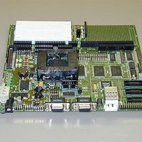
Manufacturer Part Number
MPC566EVB
Description
KIT EVALUATION FOR MPC565/566
Manufacturer
Freescale Semiconductor
Specifications of MPC566EVB
Processor To Be Evaluated
MPC56x
Data Bus Width
32 bit
Interface Type
RS-232, Ethernet
Lead Free Status / RoHS Status
Contains lead / RoHS non-compliant


Freescale Semiconductor, Inc.
System Memory
may erase or corrupt the debug monitor. If the debug monitor becomes corrupted and it’s operation
is desired, the firmware must be programmed into the flash by applying a development port tool
such as BDM or Nexus. User should use caution to avoid this situation. The upper 1 MByte is used
to store the MPC566EVB dBUG debugger/monitor firmware (0x0090_0000 to 0x009F_FFFF).
1.2.2 SRAM
The MPC566EVB has two 512 KByte device on the board (U2). It’s starting address is
0xFFF0_0000.
The synchronous SRAM Memory Bank is composed of two128K x 32 memory devices. These
memory devices are connected in linear order from U2 to U3 if more than one is available, so that
the low order address of the memory bank will access U2 and the high order addresses of the
memory bank will access U3. This memory bank must be configured as a 32 bit wide port but is
byte, half word, and word accessible for read or write operations.
Also see Section 1.2.5, “MPC566EVB Memory Map”.
1.2.3 Internal SRAM
The MPC566 processor has 36-KBtyes of internal memory which may be used as data or
instruction memory. This memory is mapped to 0x003F_8000 and configured as data space but is
not used by the dBUG monitor except during system initialization. After system initialization is
complete, the internal memory is available to the user. The memory is relocatable to any 32-KByte
boundary.
1.2.4 Internal Flash
The MPC566 has a U-bus CDR3 flash EEPROM module (UC3F). The primary function of the
UC3F flash EEPROM module is to serve as electrically programmable and erasable non-volitle
memory (NVM) to store program instructions and/or data. The MPC566 flash EEPROM array has
1 Mbytes of NVM that is divided into sixteen 64-Kbyte array blocks. If the flash array is disabled
in the IMMR register (FLEN=0), then neither the UC3F array or the UC3F control registers are
accessible. This feature allows the MPC566 to emulate the MPC561/562.
Please refer to the MPC566 User’s Manual for more details.
1.2.5 MPC566EVB Memory Map
Interface signals to support interface to external memory and peripheral devices are generated by
the memory controller. It supports four regions on four chip-select pins. The general purpose
chip-selects are available on lines CS[0] through CS[3]. CS[0] also functions as the global (boot)
chip-select for booting out of external flash.
Since the MPC566 chip selects are fully programmable, the memory banks can be located at any
location in the MPC5xx memory space.
MPC566EVB User’s Manual
1-5
For More Information On This Product,
Go to: www.freescale.com
Related parts for MPC566EVB
Image
Part Number
Description
Manufacturer
Datasheet
Request
R

Part Number:
Description:
Manufacturer:
Freescale Semiconductor, Inc
Datasheet:
Part Number:
Description:
Manufacturer:
Freescale Semiconductor, Inc
Datasheet:
Part Number:
Description:
Manufacturer:
Freescale Semiconductor, Inc
Datasheet:
Part Number:
Description:
Manufacturer:
Freescale Semiconductor, Inc
Datasheet:
Part Number:
Description:
Manufacturer:
Freescale Semiconductor, Inc
Datasheet:
Part Number:
Description:
Manufacturer:
Freescale Semiconductor, Inc
Datasheet:
Part Number:
Description:
Manufacturer:
Freescale Semiconductor, Inc
Datasheet:
Part Number:
Description:
Manufacturer:
Freescale Semiconductor, Inc
Datasheet:
Part Number:
Description:
Manufacturer:
Freescale Semiconductor, Inc
Datasheet:
Part Number:
Description:
Manufacturer:
Freescale Semiconductor, Inc
Datasheet:
Part Number:
Description:
Manufacturer:
Freescale Semiconductor, Inc
Datasheet:
Part Number:
Description:
Manufacturer:
Freescale Semiconductor, Inc
Datasheet:
Part Number:
Description:
Manufacturer:
Freescale Semiconductor, Inc
Datasheet:
Part Number:
Description:
Manufacturer:
Freescale Semiconductor, Inc
Datasheet:
Part Number:
Description:
Manufacturer:
Freescale Semiconductor, Inc
Datasheet: