EVAL-AD7687CB Analog Devices Inc, EVAL-AD7687CB Datasheet - Page 8
EVAL-AD7687CB
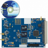
Manufacturer Part Number
EVAL-AD7687CB
Description
BOARD EVAL FOR AD7687
Manufacturer
Analog Devices Inc
Series
PulSAR®r
Specifications of EVAL-AD7687CB
Number Of Adc's
1
Number Of Bits
16
Sampling Rate (per Second)
250k
Data Interface
Serial
Inputs Per Adc
1 Differential
Input Range
±VREF
Power (typ) @ Conditions
4mW @ 5 V, 100kSPS
Voltage Supply Source
Single
Operating Temperature
-40°C ~ 85°C
Utilized Ic / Part
AD7687
Lead Free Status / RoHS Status
Contains lead / RoHS non-compliant
Other names
Q2106448


AD7687
PIN CONFIGURATIONS AND FUNCTION DESCRIPTIONS
Table 8. Pin Function Descriptions
Pin No.
1
2
3
4
5
6
7
8
9
10
1
AI = Analog Input, DI = Digital Input, DO = Digital Output, P = Power, and N/A = not applicable.
Mnemonic
REF
VDD
IN+
IN−
GND
CNV
SDO
SCK
SDI
VIO
EPAD
Figure 5. 10-Lead MSOP Pin Configuration
GND
VDD
REF
IN+
IN–
1
2
3
4
5
(Not to Scale)
Type
AI
P
AI
AI
P
DI
DO
DI
DI
P
N/A
AD7687
TOP VIEW
1
Function
Reference Input Voltage. The REF range is from 0.5 V to VDD. It is referred to the GND pin. This pin should
be decoupled closely to the pin with a 10 μF capacitor.
Power Supply.
Differential Positive Analog Input.
Differential Negative Analog Input.
Power Supply Ground.
Convert Input. This input has multiple functions. On its leading edge, it initiates the conversions and
selects the interface mode, chain or CS . In CS mode, it enables the SDO pin when low. In chain mode, the
data should be read when CNV is high.
Serial Data Output. The conversion result is output on this pin. It is synchronized to SCK.
Serial Data Clock Input. When the part is selected, the conversion result is shifted out by this clock.
Serial Data Input. This input provides multiple features. It selects the interface mode of the ADC as follows:
Chain mode is selected if SDI is low during the CNV rising edge. In this mode, SDI is used as a data input to
daisy chain the conversion results of two or more ADCs onto a single SDO line. The digital data level on
SDI is output on SDO with a delay of 16 SCK cycles.
CS mode is selected if SDI is high during the CNV rising edge. In this mode, either SDI or CNV can enable
the serial output signals when low, and if SDI or CNV is low when the conversion is complete, the BUSY
indicator feature is enabled.
Input/Output Interface Digital Power. Nominally at the same supply as the host interface (1.8 V, 2.5 V, 3 V,
or 5 V).
For the LFCSP package only, the exposed paddle must be connected to GND.
10
9
8
7
6
VIO
SDI
SCK
SDO
CNV
Rev. A | Page 8 of 28
Figure 6. 10-Lead QFN (LFCSP) Pin Configuration
GND
NOTES
1. FOR THE LFCSP PACKAGE ONLY,
VDD
REF
IN+
IN–
THE EXPOSED PADDLE MUST BE
CONNECTED TO GND.
1
2
3
4
5
(Not to Scale)
TOP VIEW
AD7687
10 VIO
9 SDI
8 SCK
7 SDO
6 CNV
Related parts for EVAL-AD7687CB
Image
Part Number
Description
Manufacturer
Datasheet
Request
R

Part Number:
Description:
ENERCHIP CC EVAL KIT
Manufacturer:
Cymbet Corporation
Datasheet:

Part Number:
Description:
BOARD EVAL FOR AD976
Manufacturer:
Analog Devices Inc
Datasheet:

Part Number:
Description:
BOARD EVAL FOR ADXL345
Manufacturer:
Analog Devices Inc
Datasheet:

Part Number:
Description:
ENERCHIP CC SEH EVAL KIT
Manufacturer:
Cymbet Corporation
Datasheet:

Part Number:
Description:
ENERCHIP EP ENERGY HARVEST EVAL
Manufacturer:
Cymbet Corporation
Datasheet:

Part Number:
Description:
EVAL BOARD FOR TW6864-LB2-GR
Manufacturer:
Intersil
Datasheet:
Part Number:
Description:
EVAL BOARD FOR TW8816-LB3-GR
Manufacturer:
Intersil
Datasheet:
Part Number:
Description:
EVAL BOARD FOR TW8817-TA3-GRS
Manufacturer:
Intersil
Datasheet:

Part Number:
Description:
EVALUATION MODULE FOR ADUM4160
Manufacturer:
Analog Devices Inc
Datasheet:

Part Number:
Description:
BOARD EVALUATION ADCMP581BCP
Manufacturer:
Analog Devices Inc
Datasheet:
Part Number:
Description:
BOARD EVALUATION ADM1041
Manufacturer:
Analog Devices Inc
Datasheet:

Part Number:
Description:
EVAL BOARD FOR STM32F107VCT
Manufacturer:
STMicroelectronics
Datasheet:
Part Number:
Description:
BOARD EVAL FOR AD1954
Manufacturer:
Analog Devices Inc
Datasheet:
Part Number:
Description:
BOARD EVAL FOR AD1955
Manufacturer:
Analog Devices Inc
Datasheet:

Part Number:
Description:
BOARD EVAL FOR AD7655
Manufacturer:
Analog Devices Inc
Datasheet: