EVAL-AD7687CB Analog Devices Inc, EVAL-AD7687CB Datasheet - Page 20
EVAL-AD7687CB
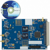
Manufacturer Part Number
EVAL-AD7687CB
Description
BOARD EVAL FOR AD7687
Manufacturer
Analog Devices Inc
Series
PulSAR®r
Specifications of EVAL-AD7687CB
Number Of Adc's
1
Number Of Bits
16
Sampling Rate (per Second)
250k
Data Interface
Serial
Inputs Per Adc
1 Differential
Input Range
±VREF
Power (typ) @ Conditions
4mW @ 5 V, 100kSPS
Voltage Supply Source
Single
Operating Temperature
-40°C ~ 85°C
Utilized Ic / Part
AD7687
Lead Free Status / RoHS Status
Contains lead / RoHS non-compliant
Other names
Q2106448


AD7687
CS MODE 4-WIRE, NO BUSY INDICATOR
This mode is usually used when multiple AD7687s are
connected to an SPI-compatible digital host.
A connection diagram example using two AD7687s is shown in
Figure 39 and the corresponding timing is given in Figure 40.
With SDI high, a rising edge on CNV initiates a conversion,
selects the CS mode, and forces SDO to high impedance. In this
mode, CNV must be held high during the conversion phase and
the subsequent data readback (if SDI and CNV are low, SDO is
driven low). Prior to the minimum conversion time, SDI could
be used to select other SPI devices, such as analog multiplexers,
but SDI must be returned high before the minimum conversion
SDI(CS1)
SDI(CS2)
ACQUISITION
CNV
SCK
SDO
t
SSDICNV
t
HSDICNV
CONVERSION
t
CONV
t
EN
SDI
AD7687
CNV
SCK
D15
1
t
HSDO
Figure 40. CS Mode 4-Wire, No BUSY Indicator Serial Interface Timing
Figure 39. CS Mode 4-Wire, No BUSY Indicator Connection Diagram
SDO
D14
2
D13
3
t
DSDO
t
SCKL
t
SCKH
Rev. A | Page 20 of 28
14
SDI
t
SCK
AD7687
15
D1
CNV
SCK
t
CYC
time and held high until the maximum conversion time to
avoid the generation of the BUSY signal indicator. When the
conversion is complete, the AD7687 enters the acquisition
phase and powers down. Each ADC result can be read by
bringing low its SDI input which consequently outputs the MSB
onto SDO. The remaining data bits are then clocked by
subsequent SCK falling edges. The data is valid on both SCK
edges. Although the rising edge can be used to capture the data,
a digital host using the SCK falling edge allows a faster reading
rate provided it has an acceptable hold time. After the 16th SCK
falling edge, or when SDI goes high, whichever is earlier, SDO
returns to high impedance and another AD7687 can be read.
16
D0
ACQUISITION
SDO
t
ACQ
D15
17
CS2
CS1
CONVERT
DATA IN
CLK
DIGITAL HOST
D14
18
30
31
D1
32
D0
t
DIS
Related parts for EVAL-AD7687CB
Image
Part Number
Description
Manufacturer
Datasheet
Request
R

Part Number:
Description:
ENERCHIP CC EVAL KIT
Manufacturer:
Cymbet Corporation
Datasheet:

Part Number:
Description:
BOARD EVAL FOR AD976
Manufacturer:
Analog Devices Inc
Datasheet:

Part Number:
Description:
BOARD EVAL FOR ADXL345
Manufacturer:
Analog Devices Inc
Datasheet:

Part Number:
Description:
ENERCHIP CC SEH EVAL KIT
Manufacturer:
Cymbet Corporation
Datasheet:

Part Number:
Description:
ENERCHIP EP ENERGY HARVEST EVAL
Manufacturer:
Cymbet Corporation
Datasheet:

Part Number:
Description:
EVAL BOARD FOR TW6864-LB2-GR
Manufacturer:
Intersil
Datasheet:
Part Number:
Description:
EVAL BOARD FOR TW8816-LB3-GR
Manufacturer:
Intersil
Datasheet:
Part Number:
Description:
EVAL BOARD FOR TW8817-TA3-GRS
Manufacturer:
Intersil
Datasheet:

Part Number:
Description:
EVALUATION MODULE FOR ADUM4160
Manufacturer:
Analog Devices Inc
Datasheet:

Part Number:
Description:
BOARD EVALUATION ADCMP581BCP
Manufacturer:
Analog Devices Inc
Datasheet:
Part Number:
Description:
BOARD EVALUATION ADM1041
Manufacturer:
Analog Devices Inc
Datasheet:

Part Number:
Description:
EVAL BOARD FOR STM32F107VCT
Manufacturer:
STMicroelectronics
Datasheet:
Part Number:
Description:
BOARD EVAL FOR AD1954
Manufacturer:
Analog Devices Inc
Datasheet:
Part Number:
Description:
BOARD EVAL FOR AD1955
Manufacturer:
Analog Devices Inc
Datasheet:

Part Number:
Description:
BOARD EVAL FOR AD7655
Manufacturer:
Analog Devices Inc
Datasheet: