CLC730132/NOPB National Semiconductor, CLC730132/NOPB Datasheet - Page 19
CLC730132/NOPB
Manufacturer Part Number
CLC730132/NOPB
Description
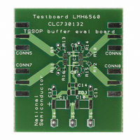
EVAL BOARD FOR THE LMH6560MT
Manufacturer
National Semiconductor
Specifications of CLC730132/NOPB
Channels Per Ic
4 - Quad
Amplifier Type
Buffer
Board Type
Bare (Unpopulated)
Utilized Ic / Part
LMH6560
Lead Free Status / RoHS Status
Lead free / RoHS Compliant
Operating Temperature
-
Output Type
-
Current - Output / Channel
-
Voltage - Supply, Single/dual (±)
-
-3db Bandwidth
-
Slew Rate
-
Current - Supply (main Ic)
-
Other names
*CLC730132
*CLC730132/NOPB
CLC730132
*CLC730132/NOPB
CLC730132


Application Notes
This effect works to both sides because the circuit will not
generate radiation but the circuit is also not sensible if ex-
posed to a certain radiation level. The same is also notice-
able when placing components flat on the printed circuit
board. Standard through hole components when placed up-
right can act as antennae causing electric fields which can
be picked up by a nearby upright component. If placed
directly at the surface of the pcb this influence is much lower.
The Effect of Variation For e
When using pcb material the e
used frequency spectrum, so if it is necessary to work with
very accurate trace impedances, one must take into account
the frequency region for which the design is to be functional.
Figure 14 http://www.isola.de gives an example of what the
drift in e
Isola. If working at frequencies of 100MHz then a 50Ω trace
has a width of 3.04mm for standard 1.6mm FR4 pcb mate-
rial, and the same trace needs a width of 3.14mm. for
frequencies around 10GHz.
Routing Power Traces
Power line traces routed over a pcb should be kept together
for best practice. If not a ground loop will occur which may
cause more sensitivity to radiation. Also additional ground
trace length may lead to more ringing on digital signals.
Careful attention to power line distribution leads to improved
r
will be when using the pcb material produced by
FIGURE 13.
FIGURE 14.
r
r
has a certain shift over the
(Continued)
20064256
20064257
19
overall circuit performance. This is especially valid for analog
circuits which are more sensitive to spurious noise and other
unwanted signals.
As demonstrated in Figure 15 the power lines are routed
from both sides on the pcb. In this case a current loop is
created as indicated by the dotted line. This loop can act as
an antenna for high frequency signals which makes the
circuit sensitive to R
power traces can be seen in the following setup. (see Figure
16).
In this arrangement the power lines have been routed in
order to avoid ground loops and to minimize sensitivity to
noise etc. The same technique is valid when routing a high
frequent signal over a board which has no ground plane. In
that case is it good practice to route the high frequency
signal alongside a ground trace. A still better way to create a
pcb carrying high frequency signals is to use a pcb with
ground a ground plane or planes.
F
radiation. A better way to route the
FIGURE 15.
FIGURE 16.
www.national.com
20064258
20064259
Related parts for CLC730132/NOPB
Image
Part Number
Description
Manufacturer
Datasheet
Request
R

Part Number:
Description:
National Semiconductor [8-Bit D/A Converter]
Manufacturer:
National Semiconductor
Datasheet:
Part Number:
Description:
National Semiconductor [Media Coprocessor]
Manufacturer:
National Semiconductor
Datasheet:
Part Number:
Description:
Digitally Controlled Tone and Volume Circuit with Stereo Audio Power Amplifier, Microphone Preamp Stage and National 3D Sound
Manufacturer:
National Semiconductor
Datasheet:
Part Number:
Description:
Digitally Controlled Tone and Volume Circuit with Stereo Audio Power Amplifier, Microphone Preamp Stage and National 3D Sound
Manufacturer:
National Semiconductor
Datasheet:
Part Number:
Description:
AC97 Rev 2 Codec with Sample Rate Conversion and National 3D Sound
Manufacturer:
National Semiconductor
Part Number:
Description:
Manufacturer:
National Semiconductor
Datasheet:
Part Number:
Description:
Manufacturer:
National Semiconductor
Datasheet:
Part Number:
Description:
General Purpose, Low Voltage, Low Power, Rail-to-Rail Output Operational Amplifiers
Manufacturer:
National Semiconductor
Datasheet:
Part Number:
Description:
8-bit 20 MSPS flash A/D converter.
Manufacturer:
National Semiconductor
Datasheet:
Part Number:
Description:
Low Noise Quad Operational Amplifier
Manufacturer:
National Semiconductor
Datasheet:
Part Number:
Description:
Quad Differential Line Receivers
Manufacturer:
National Semiconductor
Datasheet:
Part Number:
Description:
Quad High Speed Trapezoidal? Bus Transceiver
Manufacturer:
National Semiconductor
Datasheet:
Part Number:
Description:
Dual Line Receiver
Manufacturer:
National Semiconductor
Datasheet:
Part Number:
Description:
TTL to 10k ECL Level Translator with Latch
Manufacturer:
National Semiconductor
Datasheet: