© 2003 National Semiconductor Corporation
General Description
The CLC730145 and the CLC730132 evaluation boards are
designed to aid in the characterization of National Semicon-
ductor’s High Speed SOIC and TSSOP buffers. Use these
evaluation boards as a guide for high frequency layout and
as a tool to aid in device testing and characterization. The
evaluation boards schematic are shown in Figure 1 and
Figure 2. Refer to the product data sheets for recommenda-
tions for component values.
Basic Operation
These boards are a very straight forward design and are
intended to evaluate the parts behavior by offering 50Ω
inputs and outputs traces for connection to coaxial cables
with the same impedance. For other impedances the termi-
nating resistors can be modified to help match different
impedances. Both board and part are designed to handle
very high frequencies. By changing the resistor connected to
the input pin and ground the input impedance can be
matched but keep in mind that the input trace is designed for
50Ω. By using e.g. 75Ω impedance, the results will be no-
ticeably different especially for the highest frequencies. Also
at the output it is possible to match different impedances but
the output trace is designed for 50Ω. With the series resistor
at the output the output cable can be matched, however this
is not necessary. It is absolutely necessary to have the
impedance at the end of the connected cable matched to the
cable impedance but not the resistor at the beginning. Hav-
ing the output series resistor matched to the cable imped-
ance gives only an additional attenuation of −6dB. The SMA
connectors are optimized for 50Ω operation. Even with opti-
mal layout, board parasitics play a large part in high fre-
quency performance and different termination resistors will
change the frequency of the dominant parasitic poles/zeros.
Layout Considerations
Printed circuit board layout and supply bypassing play major
roles in determining high frequency performance. When de-
signing your own board use these evaluation boards as a
guide and follow these steps to optimize high frequency
performance:
• Use a ground plane
• Include large (10µF) capacitors on both supplies.
• Near the device use 10nF ceramic capacitors from both
• Near the device use a 0.1µF ceramic capacitor between
supplies to ground.
the supplies.
Quad High-Speed Buffer Evaluation Boards
CLC730145, CLC730132 (SOIC and TSSOP)
MS200709
• Minimize all trace lengths
• Terminated always all transmission lines used.
The capacitor between both supplies is recommended for
best 2nd Harmonic Distortion performance. The zenerdiode
between both supplies protect the device from reverse po-
larity supply connections under the condition these supplies
have the current limitation on. Most high-speed buffers per-
form best with capacitive loads if a small resistor is used in
series between the amplifier and the capacitor. In that case,
change the output series resistor to a value of about 10Ω
and evaluate what the output signal will do. Determine the
right value by trial and error. While using rather high capaci-
tive loads the matching at the output become less important
because the frequency response will be dramatically lower,
so a flat response will be more important. See the part’s
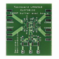
datasheets for recommended values. Sample artwork for the
CLC730145 and the CLC730132 Evaluation boards is in-
cluded on Figure 3.
Measurement Hints
The test board offers the customer two channels out of the
four buffers connected to SMA connectors. This includes the
possibility for doing measurements on cross talk and gain
matching. Furthermore it is not recommended to use normal
oscilloscope probes to test these circuits, especially when
measuring the highest frequency regions the part is active.
The capacitive loading will change circuit performance dras-
tically. Instead use high frequency low ohmic passive
probes. These probes have a load resistance in the range of
several hundred ohms until some kΩ. For best performance
use ground leads as short as possible otherwise ringing on
pulse shaped signals will occur. The use of active probes
gives also good results if basic rules are obtained, such as
the short ground leads. Another good idea to isolate the load
from the device is to change the output series resistor to a
value of 450Ω. While measuring with a coaxial cable in a
50Ω system an attenuation of 10x (20dB) will occur and this
acts as a resistive probe of 10:1. Even the best probes will
interfere with circuit operation to some degree. Also, tools,
power cables, fingers etc. near the device will change mea-
surement results. If the circuit has a good layout and there-
fore exhibits a stable behavior the measurement results will
only slightly changed by e.g. a fingertip on the circuit. If
measurement results will change dramatically it is likely the
circuit exhibits oscillations or other unwanted behavior.
www.national.com
April 2003