CLC730132/NOPB National Semiconductor, CLC730132/NOPB Datasheet - Page 18
CLC730132/NOPB
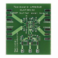
Manufacturer Part Number
CLC730132/NOPB
Description
EVAL BOARD FOR THE LMH6560MT
Manufacturer
National Semiconductor
Specifications of CLC730132/NOPB
Channels Per Ic
4 - Quad
Amplifier Type
Buffer
Board Type
Bare (Unpopulated)
Utilized Ic / Part
LMH6560
Lead Free Status / RoHS Status
Lead free / RoHS Compliant
Operating Temperature
-
Output Type
-
Current - Output / Channel
-
Voltage - Supply, Single/dual (±)
-
-3db Bandwidth
-
Slew Rate
-
Current - Supply (main Ic)
-
Other names
*CLC730132
*CLC730132/NOPB
CLC730132
*CLC730132/NOPB
CLC730132


www.national.com
Application Notes
noticeable. This causes a distinctive dip in the output fre-
quency sweep and this dip varies depending upon the par-
ticular capacitor as seen in Figure 10.
To minimize peaking due to C
purpose of isolation from the output stage should be used. A
low valued resistor will minimize the influence of such a load
capacitor. In a 50Ω system as is common in high frequency
circuits a 50Ω series resistor is often used. Usage of the
series resistor, as seen in Figure 11 eliminates the peaking
but not the dip. The dip will vary with the particular capacitor.
Using a resistor in series with a capacitor creates a rolloff of
6db/octave. Choice of a higher valued resistor, for example
500Ω to 1kΩ, and a capacitor of hundreds of pf’s provides
the expected response at lower frequencies. However, at
high frequencies the internal inductance is appreciable and
forms with the capacitor a series LC combination.
FIGURE 10.
FIGURE 11.
L
(Continued)
a series resistor for the
20064252
20064251
18
USING GROUND PLANES
A ground plane on a printed circuit board provides for a low
ohmic connection everywhere on the board for use in con-
necting supply voltages or grounds. Multilayer boards often
make use of inner conductive layers for routing supply volt-
ages. These supply voltage layers form a complete plane
rather than using discrete traces to connect the different
points together for the specified supply. Signal traces on the
other hand are routed on outside layers both top and bottom.
This allows for easy access for measurement purposes.
Fortunately, only very high density boards have signal layers
in the middle of the board. In an earlier section, the formula
for Z was derived as:
The width of a trace is determined by the thickness of the
board. In the case of a multilayer board the thickness is the
space between the trace and the first supply plane under this
trace layer. By common practice, layers do not have to be
evenly divided in the construction of a pcb. Refer to Figure
12. The design of a transmission line design over a pcb is
based upon the thickness of the different internal layers and
the er of the board material. The pcb manufacturer can
supply information about important specifications. For ex-
ample, a nominal 1.6mm thick pcb produces a 50Ω trace for
a calculated width of 2.9mm. If this layer has a thickness of
0.35mm and for the same er, the trace width for 50Ω should
be of 0.63mm, as calculated from Equation 7, a derivation
from Equation 6.
Using a trace over a ground plane has big advantages over
the use of a standard single or double sided board. The main
advantage is that the electric field generated by the signal
transported over this trace is fixed between the trace and the
ground plane e.g. there is almost no possibility of radiation.
FIGURE 12.
20064255
(6)
(7)
Related parts for CLC730132/NOPB
Image
Part Number
Description
Manufacturer
Datasheet
Request
R

Part Number:
Description:
National Semiconductor [8-Bit D/A Converter]
Manufacturer:
National Semiconductor
Datasheet:
Part Number:
Description:
National Semiconductor [Media Coprocessor]
Manufacturer:
National Semiconductor
Datasheet:
Part Number:
Description:
Digitally Controlled Tone and Volume Circuit with Stereo Audio Power Amplifier, Microphone Preamp Stage and National 3D Sound
Manufacturer:
National Semiconductor
Datasheet:
Part Number:
Description:
Digitally Controlled Tone and Volume Circuit with Stereo Audio Power Amplifier, Microphone Preamp Stage and National 3D Sound
Manufacturer:
National Semiconductor
Datasheet:
Part Number:
Description:
AC97 Rev 2 Codec with Sample Rate Conversion and National 3D Sound
Manufacturer:
National Semiconductor
Part Number:
Description:
Manufacturer:
National Semiconductor
Datasheet:
Part Number:
Description:
Manufacturer:
National Semiconductor
Datasheet:
Part Number:
Description:
General Purpose, Low Voltage, Low Power, Rail-to-Rail Output Operational Amplifiers
Manufacturer:
National Semiconductor
Datasheet:
Part Number:
Description:
8-bit 20 MSPS flash A/D converter.
Manufacturer:
National Semiconductor
Datasheet:
Part Number:
Description:
Low Noise Quad Operational Amplifier
Manufacturer:
National Semiconductor
Datasheet:
Part Number:
Description:
Quad Differential Line Receivers
Manufacturer:
National Semiconductor
Datasheet:
Part Number:
Description:
Quad High Speed Trapezoidal? Bus Transceiver
Manufacturer:
National Semiconductor
Datasheet:
Part Number:
Description:
Dual Line Receiver
Manufacturer:
National Semiconductor
Datasheet:
Part Number:
Description:
TTL to 10k ECL Level Translator with Latch
Manufacturer:
National Semiconductor
Datasheet: