CLC730132/NOPB National Semiconductor, CLC730132/NOPB Datasheet
CLC730132/NOPB
Specifications of CLC730132/NOPB
*CLC730132/NOPB
CLC730132


Related parts for CLC730132/NOPB

CLC730132/NOPB Summary of contents
Page 1
... LMH6560 well suited for the buffering of video signals. The device is fabricated on National’s high speed VIP10 process using National’s proven high performance circuit architectures. Typical Schematic LMH is a trademark of National Semiconductor Corporation. ™ © 2004 National Semiconductor Corporation Features n Closed-loop quad buffer n 680MHz small signal bandwidth n 3100V/µ ...
Page 2
... Absolute Maximum Ratings If Military/Aerospace specified devices are required, please contact the National Semiconductor Sales Office/ Distributors for availability and specifications. ESD Tolerance Human Body Model Machine Model Output Short Circuit Duration + − Supply Voltage (V –V ) Voltage at Input/Output Pins Soldering Information Infrared or Convection (20 sec.) ± ...
Page 3
Electrical Characteristics Unless otherwise specified, all limits guaranteed for T Boldface limits apply at the temperature extremes. Symbol Parameter I Input Bias Current Temperature Coefficient Input B Bias Current R Output Resistance OUT PSRR Power ...
Page 4
Electrical Characteristics Unless otherwise specified, all limits guaranteed for T Boldface limits apply at the temperature extremes. Symbol Parameter Distortion And Noise Performance nd HD2 2 Harmonic Distortion rd HD3 3 Harmonic Distortion THD Total Harmonic Distortion e Input-Referred ...
Page 5
Electrical Characteristics Unless otherwise specified, all limits guaranteed for T Boldface limits apply at the temperature extremes. Symbol Parameter Frequency Domain Response SSBW Small Signal Bandwidth < GFN Gain Flatness 0.1dB FPBW Full Power Bandwidth (−3dB) Time Domain Response ...
Page 6
Electrical Characteristics Unless otherwise specified, all limits guaranteed for T Boldface limits apply at the temperature extremes. Symbol Parameter V Output Swing Positive O Output Swing Negative I Output Short Circuit Current SC I Linear Output Current O Note ...
Page 7
Connection Diagram Ordering Information Package Part Number 14-pin SOIC LMH6560MA LMH6560MAX 14-pin TSSOP LMH6560MT LMH6560MTX 14-Pin SOIC/TSSOP 20064234 Top View Package Marking Transport Media LMH6560MA 55 Units/Rail 2.5k Units Tape and Reel LMH6560MT 94 Units/Rail 2.5k Units Tape and Reel ...
Page 8
Typical Performance Characteristics fied. Frequency Response Gain Flatness 0.1dB Differential Gain and Phase www.national.com + 25˚ +5V Frequency Response Over Temperature 20064206 Differential Gain and Phase 20064208 Transient Response Positive 20064205 8 − ...
Page 9
Typical Performance Characteristics specified. (Continued) Transient Response Negative Transient Response Negative for Various V Harmonic Distortion vs. V OUT + 25˚ +5V Transient Response Positive for Various V 20064226 Harmonic Distortion vs. V ...
Page 10
Typical Performance Characteristics specified. (Continued) THD vs. V for Various Frequencies OUT Linearity V vs. V OUT Crosstalk vs. Time www.national.com + 25˚ +5V 20064224 IN 20064220 20064203 10 − = −5V; unless ...
Page 11
Typical Performance Characteristics specified. (Continued) V vs. V for Unit 1 OS SUPPLY V vs. V for Unit 3 OS SUPPLY R vs. Frequency OUT + 25˚ +5V vs 20064231 ...
Page 12
Typical Performance Characteristics specified. (Continued) I vs. V SUPPLY SUPPLY V vs. I (Sinking) OUT OUT I Sinking vs. V OUT www.national.com 25˚ 20064216 20064215 SUPPLY 20064213 12 + − = +5V −5V; ...
Page 13
Typical Performance Characteristics specified. (Continued) Small Signal Pulse Response Large Signal Pulse Response + 25˚ +5V Large Signal Pulse Response 20064223 @ Large Signal Pulse Response S 20064218 13 − ...
Page 14
Application Notes USING BUFFERS A buffer is an electronic device delivering current gain but no voltage gain used in cases where low impedances need to be driven and more drive current is required. Buffers need a flat frequency ...
Page 15
Application Notes (Continued) FIGURE 4. Z can be calculated by knowing some of the physical di- 0 mensions of the pcb line, such as pcb thickness, width of the trace and e , relative dielectric constant. The formula given in ...
Page 16
Application Notes (Continued) The voltage wavefront of 2.45V will now set about traveling back over the transmission line towards the source, thereby resulting in a reflection caused by the mismatch. On the other hand if the load is less then ...
Page 17
Application Notes (Continued) termination resistor, provided the termination value is Z wavefront undergoes total absorption by the termination. This is only true if the output impedance of the buffer/driver is low in comparison to the characteristic impedance Z this moment ...
Page 18
Application Notes (Continued) noticeable. This causes a distinctive dip in the output fre- quency sweep and this dip varies depending upon the par- ticular capacitor as seen in Figure 10. FIGURE 10. To minimize peaking due series ...
Page 19
Application Notes (Continued) FIGURE 13. This effect works to both sides because the circuit will not generate radiation but the circuit is also not sensible if ex- posed to a certain radiation level. The same is also notice- able when ...
Page 20
Application Notes (Continued) Discontinuities in a Ground Plane A ground plane with traces routed over this plane results in the build electric field between the trace and the ground plane as seen in Figure 13. This field ...
Page 21
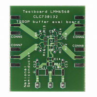
... SOIC-14 LMH6560MT TSSOP-14 These free evaluation boards are shipped when a device sample request is placed with National Semiconductor. POWER SEQUENCING OF THE LMH6560 Caution should be used in applying power to the LMH6560. When the negative power supply pin is left floating it is recommended that other pins, such as positive supply and signal input should also be left unconnected ...
Page 22
Physical Dimensions unless otherwise noted www.national.com inches (millimeters) 14-Pin SOIC NS Package Number M14A 14-Pin TSSOP NS Package Number MTC14 22 ...
Page 23
... BANNED SUBSTANCE COMPLIANCE National Semiconductor certifies that the products and packing materials meet the provisions of the Customer Products Stewardship Specification (CSP-9-111C2) and the Banned Substances and Materials of Interest Specification (CSP-9-111S2) and contain no ‘‘Banned Substances’’ as defined in CSP-9-111S2. ...