KSZ8851SNL-BBE-EVAL Micrel Inc, KSZ8851SNL-BBE-EVAL Datasheet - Page 12
KSZ8851SNL-BBE-EVAL
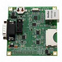
Manufacturer Part Number
KSZ8851SNL-BBE-EVAL
Description
BOARD EVAL MAC/PHY FOR KSZ8851
Manufacturer
Micrel Inc
Series
LinkMD®r
Datasheets
1.KSZ8851SNL-BBE-EVAL.pdf
(80 pages)
2.KSZ8851SNL-BBE-EVAL.pdf
(3 pages)
3.KSZ8851SNL-BBE-EVAL.pdf
(1 pages)
Specifications of KSZ8851SNL-BBE-EVAL
Design Resources
BeagleBoard Zippy2
Main Purpose
Interface, Ethernet Controller (PHY and MAC)
Embedded
No
Utilized Ic / Part
KSZ8851SNL
Primary Attributes
1 Port, 100BASE-TX/10BASE-T
Secondary Attributes
SPI Interface, LinkMD Cable Diagnostics
Lead Free Status / RoHS Status
Lead free / RoHS Compliant
Other names
576-3602
KSZ8851SNL-BBE-EVL
ZIPPY2
KSZ8851SNL-BBE-EVL
ZIPPY2
Available stocks
Company
Part Number
Manufacturer
Quantity
Price
Company:

Part Number:
KSZ8851SNL-BBE-EVAL
Manufacturer:
Micrel Inc
Quantity:
135


Legend:
P = Power supply
I/O = Bi-directional I = Input O = Output.
Ipd = Input with internal pull-down (58K +/-30%).
Ipu = Input with internal pull-up (58K +/-30%).
Opd = Output with internal pull-down (58K +/-30%).
Opu = Output with internal pull-up (58K +/-30%).
Ipu/O = Input with internal pull-up (58K +/-30%) during power-up/reset; output pin otherwise.
Ipd/O = Input with internal pull-down (58K +/-30%) during power-up/reset; output pin otherwise.
Strapping Options
Note: Ipd/O = Input with internal pull-down (58K +/-30%) during power-up/reset; output pin otherwise.
August 2009
Micrel, Inc.
Pin Number
Pin Number
Pin strap-ins are latched during power-up or reset.
20
21
22
23
24
25
26
27
28
29
30
31
32
6
Gnd = Ground
VDD_D1.8
Pin Name
Pin Name
VDD_IO
VDD_IO
EED_IO
DGND
DGND
DGND
SCLK
LED1
CSN
SO
X1
X2
SI
Ipd/O
Type
Type
Gnd
Gnd
Gnd
Opu
Ipu
Ipd
O
P
P
O
P
I
I
Pin Function
Hardware reset pin (active Low). This reset input must be held low for a minimum of 10ms
after stable supply voltage 3.3V.
25MHz crystal or oscillator clock connection.
Pins (X1, X2) connect to a crystal. If an oscillator is used, X1 connects to a 3.3V tolerant
oscillator and X2 is a no connect.
Note: Clock requirement is +/- 50ppm for either crystal or oscillator.
Digital IO ground
1.8V digital power supply from VDD_CO1.8 (pin 5) with appropriate filtering. If VDD_IO is
1.8V, this pin must be supplied power from the same source as pins 25 and 30 (VDD_IO)
with appropriate filtering.
Digital IO ground
3.3V, 2.5V or 1.8V digital V
SPI slave mode: Chip Select Not
Active low input pin for SPI interface.
SPI slave mode: Serial data out for SPI interface. This SO is tri-stated output when CSN
is negated and this pin must have external 4.7K pull-up to keep the SO line high while the
driver is tri-stated.
SPI slave mode: Serial clock input for SPI interface. This clock speed can run up to
40MHz.
Digital IO ground
3.3V, 2.5V or 1.8V digital V
SPI slave mode: Serial data in for SPI interface.
Programmable LED1 output to indicate PHY activity/status (see LED0 description at pin1)
Pin Function
EEPROM select:
Pull-up = EEPROM present
Floating (NC) or Pull-down = EEPROM not present (default)
During power-up / reset, this pin value is latched into register CCR, bit 9
12
DD
DD
input power supply for IO with well decoupling capacitors.
input power supply for IO with well decoupling capacitors.
KSZ8851SNL/SNLI
M9999-083109-2.0
Related parts for KSZ8851SNL-BBE-EVAL
Image
Part Number
Description
Manufacturer
Datasheet
Request
R

Part Number:
Description:
BOARD EVALUATION KSZ8851SNL
Manufacturer:
Micrel Inc
Datasheet:

Part Number:
Description:
IC CTLR MAC/PHY NON-PCI 32-MLF
Manufacturer:
Micrel Inc
Datasheet:

Part Number:
Description:
IC CTLR MAC/PHY NON-PCI 32-QFN
Manufacturer:
Micrel Inc
Datasheet:

Part Number:
Description:
Manufacturer:
Micrel Inc
Datasheet:
Part Number:
Description:
Manufacturer:
Micrel Inc
Datasheet:
Part Number:
Description:
Manufacturer:
Micrel Inc
Datasheet:
Part Number:
Description:
Manufacturer:
Micrel Inc
Datasheet:
Part Number:
Description:
Manufacturer:
Micrel Inc
Datasheet:
Part Number:
Description:
Manufacturer:
Micrel Inc
Datasheet:
Part Number:
Description:
Manufacturer:
Micrel Inc
Datasheet:
Part Number:
Description:
Manufacturer:
Micrel Inc
Datasheet:
Part Number:
Description:
Manufacturer:
Micrel Inc
Datasheet:
Part Number:
Description:
Manufacturer:
Micrel Inc
Datasheet:
Part Number:
Description:
Manufacturer:
Micrel Inc
Datasheet: