MA330013 Microchip Technology, MA330013 Datasheet - Page 238
MA330013
Manufacturer Part Number
MA330013
Description
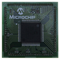
MODULE PLUG-IN DSPIC33 100TQFP
Manufacturer
Microchip Technology
Specifications of MA330013
Accessory Type
Plug-In Module (PIM) - dsPIC33FJ256MC710
Tool / Board Applications
General Purpose MCU, MPU, DSP, DSC
Mcu Supported Families
DsPIC33
Silicon Manufacturer
Microchip
Core Architecture
DsPIC
Core Sub-architecture
DsPIC33
Silicon Core Number
DsPIC33F
Silicon Family Name
DsPIC33FJxxMCxxx
Rohs Compliant
Yes
For Use With
DM330023 - BOARD DEV DSPICDEM MCHV
Lead Free Status / RoHS Status
Not applicable / Not applicable
For Use With/related Products
Explorer 16 (DM240001 or DM240002)
Lead Free Status / RoHS Status
Lead free / RoHS Compliant, Not applicable / Not applicable


dsPIC33F
20.5.7
Transmit interrupts can be divided into 2 major groups,
each including various conditions that generate
interrupts:
• Transmit Interrupt:
• Transmit Error Interrupts:
FIGURE 20-2:
DS70165E-page 236
T
- Transmitter Warning Interrupt:
- Transmitter Error Passive:
- Bus Off:
Note:
At least one of the three transmit buffers is empty
(not scheduled) and can be loaded to schedule a
message for transmission. Reading the TXnIF
flags will indicate which transmit buffer is available
and caused the interrupt.
A transmission error interrupt will be indicated by
the ERRIF flag. This flag shows that an error con-
dition occurred. The source of the error can be
determined by checking the error flags in the CAN
Interrupt Flag register, CiINTF. The flags in this
register are related to receive and transmit errors.
Input Signal
Q
The TXWAR bit indicates that the transmit error
counter has reached the CPU warning limit
of 96.
The TXEP bit (CiINTF<12>) indicates that the
transmit error counter has exceeded the error
passive limit of 127 and the module has gone to
error passive state.
The TXBO bit (CiINTF<13>) indicates that the
transmit error counter has exceeded 255 and
the module has gone to the bus off state.
TRANSMIT INTERRUPTS
Both ECAN1 and ECAN2 can trigger a
DMA data transfer. If C1TX, C1RX, C2TX
or C2RX is selected as a DMA IRQ
source, a DMA transfer occurs when the
C1TXIF, C1RXIF, C2TXIF or C2RXIF bit
gets set as a result of an ECAN1 or
ECAN2 transmission or reception.
Sync
ECAN™ MODULE BIT TIMING
Segment
Prop
Segment 1
Phase
Preliminary
Sample Point
20.6
All nodes on any particular CAN bus must have the
same nominal bit rate. In order to set the baud rate, the
following parameters have to be initialized:
• Synchronization Jump Width
• Baud Rate Prescaler
• Phase Segments
• Length Determination of Phase Segment 2
• Sample Point
• Propagation Segment bits
20.6.1
All controllers on the CAN bus must have the same
baud rate and bit length. However, different controllers
are not required to have the same master oscillator
clock. At different clock frequencies of the individual
controllers, the baud rate has to be adjusted by
adjusting the number of time quanta in each segment.
The nominal bit time can be thought of as being divided
into separate non-overlapping time segments. These
segments are shown in Figure 20-2.
• Synchronization Segment (Sync Seg)
• Propagation Time Segment (Prop Seg)
• Phase Segment 1 (Phase1 Seg)
• Phase Segment 2 (Phase2 Seg)
The time segments and also the nominal bit time are
made up of integer units of time called time quanta or
T
of 8 T
the minimum nominal bit time is 1 sec corresponding
to a maximum bit rate of 1 MHz.
Q
. By definition, the nominal bit time has a minimum
Q
and a maximum of 25 T
Baud Rate Setting
BIT TIMING
Segment 2
Phase
© 2007 Microchip Technology Inc.
Q
. Also, by definition,
Sync
Related parts for MA330013
Image
Part Number
Description
Manufacturer
Datasheet
Request
R

Part Number:
Description:
Manufacturer:
Microchip Technology Inc.
Datasheet:
Part Number:
Description:
Manufacturer:
Microchip Technology Inc.
Datasheet:
Part Number:
Description:
Manufacturer:
Microchip Technology Inc.
Datasheet:
Part Number:
Description:
Manufacturer:
Microchip Technology Inc.
Datasheet:
Part Number:
Description:
Manufacturer:
Microchip Technology Inc.
Datasheet:
Part Number:
Description:
Manufacturer:
Microchip Technology Inc.
Datasheet:
Part Number:
Description:
Manufacturer:
Microchip Technology Inc.
Datasheet:
Part Number:
Description:
Manufacturer:
Microchip Technology Inc.
Datasheet: