MA330013 Microchip Technology, MA330013 Datasheet - Page 138
MA330013
Manufacturer Part Number
MA330013
Description
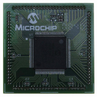
MODULE PLUG-IN DSPIC33 100TQFP
Manufacturer
Microchip Technology
Specifications of MA330013
Accessory Type
Plug-In Module (PIM) - dsPIC33FJ256MC710
Tool / Board Applications
General Purpose MCU, MPU, DSP, DSC
Mcu Supported Families
DsPIC33
Silicon Manufacturer
Microchip
Core Architecture
DsPIC
Core Sub-architecture
DsPIC33
Silicon Core Number
DsPIC33F
Silicon Family Name
DsPIC33FJxxMCxxx
Rohs Compliant
Yes
For Use With
DM330023 - BOARD DEV DSPICDEM MCHV
Lead Free Status / RoHS Status
Not applicable / Not applicable
For Use With/related Products
Explorer 16 (DM240001 or DM240002)
Lead Free Status / RoHS Status
Lead free / RoHS Compliant, Not applicable / Not applicable


dsPIC33F
FIGURE 7-1:
7.1
Each DMAC Channel x (x = 0, 1, 2, 3, 4, 5, 6 or 7)
contains the following registers:
• A 16-bit DMA Channel Control register
• A 16-bit DMA Channel IRQ Select register
• A 16-bit DMA RAM Primary Start Address register
• A 16-bit DMA RAM Secondary Start Address
• A 16-bit DMA Peripheral Address register
• A 10-bit DMA Transfer Count register (DMAx-
An additional pair of status registers, DMACS0 and
DMACS1, are common to all DMAC channels.
DMACS0 contains the DMA RAM and SFR write colli-
sion flags, XWCOLx and PWCOLx, respectively.
DMACS1 indicates DMA channel and Ping-Pong
mode status.
The
DMAxCNT are all conventional read/write registers.
Reads of DMAxSTA or DMAxSTB will read the con-
tents of the DMA RAM Address register. Writes to
DMAxSTA or DMAxSTB write to the registers. This
allows the user to determine the DMA buffer pointer
value (address) at any time.
The interrupt flags (DMAxIF) are located in an IFSx
register in the interrupt controller. The corresponding
interrupt enable control bits (DMAxIE) are located in
DS70165E-page 136
(DMAxCON)
(DMAxREQ)
(DMAxSTA)
register (DMAxSTB)
(DMAxPAD)
CNT)
Note: CPU and DMA address buses are not shown for clarity.
SRAM
DMAxCON,
DMAC Registers
SRAM X-Bus
CPU
DMAxREQ,
TOP LEVEL SYSTEM ARCHITECTURE USING A DEDICATED TRANSACTION BUS
PORT 1
DMA RAM
CPU Peripheral DS Bus
Peripheral
Non-DMA
Ready
PORT 2
DMAxPAD
DMA DS Bus
and
Preliminary
DMA Controller
an IECx register in the interrupt controller, and the cor-
responding interrupt priority control bits (DMAxIP) are
located in an IPCx register in the interrupt controller.
7.2
Each DMA channel has its own status and control reg-
ister (DMAxCON) that is used to configure the channel
to support the following operating modes:
• Word or byte size data transfers
• Peripheral to DMA RAM or DMA RAM to
• Post-increment or static DMA RAM address
• One-shot or continuous block transfers
• Auto-switch between two start addresses after
• Force a single DMA transfer (Manual mode)
Each DMA channel can be independently configured
to:
• Select from one of 20 DMA request sources
• Manually enable or disable the DMA channel
• Interrupt the CPU when the transfer is half or fully
DMA channel interrupts are routed to the interrupt con-
troller module and enabled through associated enable
flags.
The channel DMA RAM and peripheral write collision
Faults are combined into a single DMAC error trap
(Level 10) and are not maskable. Each channel has
DMA RAM write collision (XWCOLx) and peripheral
peripheral transfers
each transfer complete (Ping-Pong mode)
complete
Channels
DMA
Peripheral Indirect Address
DMAC Operating Modes
Peripheral 1
CPU
Ready
DMA
© 2007 Microchip Technology Inc.
DMA
Peripheral 3
CPU
Ready
DMA
DMA
Peripheral 2
CPU
Ready
DMA
DMA
Related parts for MA330013
Image
Part Number
Description
Manufacturer
Datasheet
Request
R

Part Number:
Description:
Manufacturer:
Microchip Technology Inc.
Datasheet:
Part Number:
Description:
Manufacturer:
Microchip Technology Inc.
Datasheet:
Part Number:
Description:
Manufacturer:
Microchip Technology Inc.
Datasheet:
Part Number:
Description:
Manufacturer:
Microchip Technology Inc.
Datasheet:
Part Number:
Description:
Manufacturer:
Microchip Technology Inc.
Datasheet:
Part Number:
Description:
Manufacturer:
Microchip Technology Inc.
Datasheet:
Part Number:
Description:
Manufacturer:
Microchip Technology Inc.
Datasheet:
Part Number:
Description:
Manufacturer:
Microchip Technology Inc.
Datasheet: