MA330013 Microchip Technology, MA330013 Datasheet - Page 182
MA330013
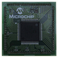
Manufacturer Part Number
MA330013
Description
MODULE PLUG-IN DSPIC33 100TQFP
Manufacturer
Microchip Technology
Specifications of MA330013
Accessory Type
Plug-In Module (PIM) - dsPIC33FJ256MC710
Tool / Board Applications
General Purpose MCU, MPU, DSP, DSC
Mcu Supported Families
DsPIC33
Silicon Manufacturer
Microchip
Core Architecture
DsPIC
Core Sub-architecture
DsPIC33
Silicon Core Number
DsPIC33F
Silicon Family Name
DsPIC33FJxxMCxxx
Rohs Compliant
Yes
For Use With
DM330023 - BOARD DEV DSPICDEM MCHV
Lead Free Status / RoHS Status
Not applicable / Not applicable
For Use With/related Products
Explorer 16 (DM240001 or DM240002)
Lead Free Status / RoHS Status
Lead free / RoHS Compliant, Not applicable / Not applicable


dsPIC33F
15.6
In the Complementary mode of operation, each pair of
PWM outputs is obtained by a complementary PWM
signal. A dead time may be optionally inserted during
device switching, when both outputs are inactive for a
short period (refer to Section 15.7 “Dead-Time
Generators”).
In Complementary mode, the duty cycle comparison
units are assigned to the PWM outputs as follows:
• PDC1 register controls PWM1H/PWM1L outputs
• PDC2 register controls PWM2H/PWM2L outputs
• PDC3 register controls PWM3H/PWM3L outputs
• PDC4 register controls PWM4H/PWM4L outputs
The Complementary mode is selected for each PWM
I/O pin pair by clearing the appropriate PMODx bit in the
PWMCON1 SFR. The PWM I/O pins are set to
Complementary mode by default upon a device Reset.
15.7
Dead-time generation may be provided when any of the
PWM I/O pin pairs are operating in the Complementary
Output mode. The PWM outputs use push-pull drive cir-
cuits. Due to the inability of the power output devices to
switch instantaneously, some amount of time must be
provided between the turn-off event of one PWM output
in a complementary pair and the turn-on event of the
other transistor.
FIGURE 15-4:
DS70165E-page 180
Complementary PWM Operation
Dead-Time Generators
Duty Cycle Generator
PWMxH
PWMxL
Time Selected by DTSxA bit (A or B)
DEAD-TIME TIMING DIAGRAM
Preliminary
The PWM module allows two different dead times to be
programmed. These two dead times may be used in
one of two methods, described below, to increase user
flexibility:
• The PWM output signals can be optimized for
• The two dead times can be assigned to individual
15.7.1
Each complementary output pair for the PWM module
has a 6-bit down counter that is used to produce the
dead-time insertion. As shown in Figure 15-4, each
dead-time unit has a rising and falling edge detector
connected to the duty cycle comparison output.
different turn-off times in the high side and low
side transistors in a complementary pair of tran-
sistors. The first dead time is inserted between
the turn-off event of the lower transistor of the
complementary pair and the turn-on event of the
upper transistor. The second dead time is inserted
between the turn-off event of the upper transistor
and the turn-on event of the lower transistor.
PWM I/O pin pairs. This operating mode allows
the PWM module to drive different transistor/load
combinations with each complementary PWM I/O
pin pair.
DEAD-TIME GENERATORS
Time Selected by DTSxI bit (A or B)
© 2007 Microchip Technology Inc.
Related parts for MA330013
Image
Part Number
Description
Manufacturer
Datasheet
Request
R

Part Number:
Description:
Manufacturer:
Microchip Technology Inc.
Datasheet:
Part Number:
Description:
Manufacturer:
Microchip Technology Inc.
Datasheet:
Part Number:
Description:
Manufacturer:
Microchip Technology Inc.
Datasheet:
Part Number:
Description:
Manufacturer:
Microchip Technology Inc.
Datasheet:
Part Number:
Description:
Manufacturer:
Microchip Technology Inc.
Datasheet:
Part Number:
Description:
Manufacturer:
Microchip Technology Inc.
Datasheet:
Part Number:
Description:
Manufacturer:
Microchip Technology Inc.
Datasheet:
Part Number:
Description:
Manufacturer:
Microchip Technology Inc.
Datasheet: