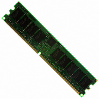
MT18VDDF12872Y-40BF1 Micron Technology Inc, MT18VDDF12872Y-40BF1 Datasheet - Page 21

MT18VDDF12872Y-40BF1
Manufacturer Part Number
MT18VDDF12872Y-40BF1
Description
MODULE DDR SDRAM 1GB 184-DIMM
Manufacturer
Micron Technology Inc
Specifications of MT18VDDF12872Y-40BF1
Memory Type
DDR SDRAM
Memory Size
1GB
Speed
400MT/s
Package / Case
184-DIMM
Main Category
DRAM Module
Sub-category
DDR SDRAM
Module Type
184RDIMM
Device Core Size
72b
Organization
128Mx72
Total Density
1GByte
Chip Density
512Mb
Access Time (max)
700ps
Maximum Clock Rate
400MHz
Operating Supply Voltage (typ)
2.6V
Operating Current
1.8A
Number Of Elements
18
Operating Supply Voltage (max)
2.7V
Operating Supply Voltage (min)
2.5V
Operating Temp Range
0C to 70C
Operating Temperature Classification
Commercial
Pin Count
184
Mounting
Socket
Lead Free Status / RoHS Status
Lead free / RoHS Compliant
Other names
557-1233
MT18VDDF12872Y-40BF1
MT18VDDF12872Y-40BF1
Initialization
tialized as described below:
pdf: 09005aef80f6b913, source: 09005aef80f6b41c
DDAF18C64_128x72G.fm - Rev. C 9/04 EN
10. Wait at least
11. Using the LMR command program the Mode Reg-
12. Wait at least
13. Issue a PRECHARGE ALL command.
14. Wait at least
15. Issue an AUTO REFRESH command (Note this
16. Wait at least
17. Issue an AUTO REFRESH command (Note this
18. Wait at least
19. Although not required by the Micron device,
20. Wait at least
21. At this point the DRAM is ready for any valid com-
1. Simultaneously apply power to V
2. Apply V
3. Assert and hold CKE at a LVCMOS logic low.
4. Provide stable CLOCK signals.
5. Wait at least 200µs.
6. Bring CKE high and provide at least one NOP or
7. Perform a PRECHARGE ALL command.
8. Wait at least
9. Using the LMR command program the Extended
To ensure device operation the DRAM must be ini-
DESELECT command. At this point the CKE input
changes from a LVCMOS input to a SSTL2 input
only and will remain a SSTL_2 input unless a
power cycle occurs.
DESELECT commands must be given.
Mode Register (E0 = 0 to enable the DLL and E1 =
0 for normal drive or E1 = 1 for reduced drive, E2
through En must be set to 0; where n = most sig-
nificant bit).
commands are allowed.
ister to set operating parameters and to reset the
DLL. Note at least 200 clock cycles are required
between a DLL reset and any READ command.
commands are allowed.
commands are allowed.
may be moved prior to step 13).
commands are allowed.
may be moved prior to step 13).
commands are allowed.
JEDEC requires a LMR command to clear the DLL
bit (set M8 = 0). If a LMR command is issued the
same operating parameters should be utilized as
in step 11.
commands are allowed.
mand. Note 200 clock cycles are required between
step 11 (DLL Reset) and any READ command.
REF
and then V
t
t
t
t
t
MRD time, only NOPs or DESELECT
MRD time, only NOPs or DESELECT
MRD time, only NOPs or DESELECT
t
t
RFC time, only NOPs or DESELECT
RFC time, only NOPs or DESELECT
RP time, during this time NOPs or
RP time, only NOPs or DESELECT
TT
power.
DD
and V
DD
Q.
21
512MB, 1GB (x72, ECC, SR) PC3200
Figure 10: Initialization Flow Diagram
Micron Technology, Inc., reserves the right to change products or specifications without notice.
184-PIN DDR SDRAM RDIMM
Step
10
11
12
13
14
15
16
17
18
19
20
21
1
2
3
4
5
6
7
8
9
Configure Load Mode Register and reset DLL
Assert NOP or DESELECT commands for t RFC
Optional LMR command to clear DLL bit
Assert NOP or DESELECT for t MRD time
Assert NOP or DESELECT for t MRD time
Assert NOP or DESELECT for t MRD time
DRAM is ready for any valid command
Assert NOP or DESELECT for t RFC time
Bring CKE High with a NOP command
Assert NOP or DESELECT for t RP time
Assert NOP or DESELECT for t RP time
Configure Extended Mode Register
Issue AUTO REFRESH command
Issue AUTO REFRESH command
CKE must be LVCMOS Low
V
Apply stable CLOCKs
Wait at least 200us
Apply V
DD
PRECHARGE ALL
PRECHARGE ALL
and V
REF
©2004 Micron Technology, Inc. All rights reserved.
DD
and V
Q Ramp
TT


