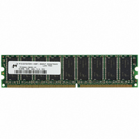
MT9VDDT6472AY-40BF1 Micron Technology Inc, MT9VDDT6472AY-40BF1 Datasheet - Page 15

MT9VDDT6472AY-40BF1
Manufacturer Part Number
MT9VDDT6472AY-40BF1
Description
MODULE DDR SDRAM 512MB 184-DIMM
Manufacturer
Micron Technology Inc
Datasheet
1.MT9VDDT6472AY-40BF1.pdf
(27 pages)
Specifications of MT9VDDT6472AY-40BF1
Memory Type
DDR SDRAM
Memory Size
512MB
Speed
400MT/s
Package / Case
184-DIMM
Lead Free Status / RoHS Status
Lead free / RoHS Compliant
Other names
557-1178
MT9VDDT6472AY-40BF1
MT9VDDT6472AY-40BF1
Table 14: I
DRAM components only
Notes: 1–5, 8, 10, 12; notes appear on pages 18–20; 0°C
pdf: 09005aef80a43e7d, source: 09005aef80a43d77
DDA9C16_32_64x72AG.fm - Rev. B 9/04 EN
OPERATING CURRENT: One device bank; Active-Precharge;
(MIN);
clock cycle; Address and control inputs changing once every two
clock cycles;
OPERATING CURRENT: One device bank; Active-Read-Precharge;
Burst = 4;
control inputs changing once per clock cycle
PRECHARGE POWER-DOWN STANDBY CURRENT: All device banks
idle; Power-down mode;
IDLE STANDBY CURRENT: CS# = HIGH; All device banks idle;
(MIN); CKE = HIGH; Address and other control inputs changing once
per clock cycle. V
ACTIVE POWER-DOWN STANDBY CURRENT: One device bank active;
Power-down mode;
ACTIVE STANDBY CURRENT: CS# = HIGH; CKE = HIGH; One device
bank; Active-Precharge;
and DQS inputs changing twice per clock cycle; Address and other
control inputs changing once per clock cycle
OPERATING CURRENT: Burst = 2; Reads; Continuous burst; One device
bank active; Address and control inputs changing once per clock
cycle;
OPERATING CURRENT: Burst = 2; Writes; Continuous burst; One
device bank active; Address and control inputs changing once per
clock cycle;
per clock cycle
AUTO REFRESH CURRENT
SELF REFRESH CURRENT: CKE
OPERATING CURRENT: Four device bank interleaving READs (BL = 4)
with auto precharge,
control inputs change only during Active, READ, or WRITE
commands.
t
CK =
t
CK =
t
RC =
t
t
CK =
CK (MIN); I
t
CK (MIN); DQ, DM, and DQS inputs changing once per
t
DD
RC (MIN);
IN
t
CK (MIN); DQ, DM, and DQS inputs changing twice
= V
t
Specifications and Conditions – 512MB
CK =
PARAMETER/CONDITION
t
RC =
REF
OUT
t
RC =
t
CK =
for DQ, DQS, and DM
t
t
CK (MIN); CKE = LOW
t
CK =
= 0mA
RC (MIN);
t
RAS (MAX);
t
0.2V
CK (MIN); CKE = LOW;
t
CK (MIN); I
t
CK =
128MB, 256MB, 512MB (x72, ECC, SR), PC3200
t
t
CK =
OUT
CK (MIN); Address and
= 0mA; Address and
t
CK (MIN); DQ, DM,
t
t
Standard
REFC =
REFC = 7.8125µs
T
A
t
RFC (MIN)
t
t
RC =
15
CK =
+70°C; V
t
RC
t
CK
DD
Micron Technology, Inc., reserves the right to change products or specifications without notice.
184-Pin DDR SDRAM UDIMM
SYMBOL
= V
I
I
I
I
I
I
I
DD 4 W
DD 3 N
DD 5A
I
I
DD 2 P
DD 3 P
DD 4 R
I
I
I
DD 2 F
DD 0
DD 1
DD 5
DD 6
DD 7
DD
Q = +2.6V ±0.1V
MAX
1,395
1,665
1,710
1,755
3,105
4,050
-40B
495
405
540
45
99
45
UNITS
mA
mA
mA
mA
mA
mA
mA
mA
mA
mA
mA
mA
©2004 Micron Technology, Inc.
21, 28, 44
21, 28, 44
NOTES
20, 42
20, 42
20, 41
20, 42
20, 44
24, 44
20, 43
45
20
9


