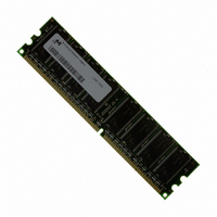
MT8VDDT6464AY-40BF4 Micron Technology Inc, MT8VDDT6464AY-40BF4 Datasheet - Page 17

MT8VDDT6464AY-40BF4
Manufacturer Part Number
MT8VDDT6464AY-40BF4
Description
MODULE DDR SDRAM 512MB 184-DIMM
Manufacturer
Micron Technology Inc
Datasheet
1.MT8VDDT6464AY-40BF4.pdf
(26 pages)
Specifications of MT8VDDT6464AY-40BF4
Memory Type
DDR SDRAM
Memory Size
512MB
Speed
400MT/s
Package / Case
184-DIMM
Lead Free Status / RoHS Status
Lead free / RoHS Compliant
Other names
557-1232
MT8VDDT6464AY-40BF4
MT8VDDT6464AY-40BF4
Figure 5:
PDF: 09005aef80a43556, Source: 09005aef80a43534
DDA8C16_32_64x64AG_2.fm - Rev. E 4/06 EN
Pull-Down Characteristics
16. This limit is actually a nominal value and does not result in a fail value. CKE is HIGH
17. To maintain a valid level, the transitioning edge of the input must:
18. V
19. Any positive glitch in the nominal voltage must be less than 1/3 of the clock and not
20. Normal Output Drive Curves:
17b. Reach at least the target AC level.
20b. The variation in driver pull-down current within nominal limits of voltage and
20d. The variation in driver pull-up current within nominal limits of voltage and tem-
17a. Sustain a constant slew rate from the current AC level through to the target AC
17c. After the AC target level is reached, continue to maintain at least the target DC
20a. The full variation in driver pull-down current from minimum to maximum pro-
20c. The full variation in driver pull-up current from minimum to maximum process,
20e. The full variation in the ratio of the maximum to minimum pull-up and pull-
160
140
120
100
20f. The full variation in the ratio of the nominal pull-up to pull-down current should
80
60
40
20
during REFRESH command period (
standby).
more than +300mV or 2.9V, whichever is less. Any negative glitch must be <1/3 of the
clock cycle and not exceed either -200mV or 2.4V, whichever is more positive.
0
0.0
DD
level, V
level, V
cess, temperature and voltage will lie within the outer bounding lines of the V-I
curve of Figure 5.
temperature is expected, but not guaranteed, to lie within the inner bounding
lines of the V-I curve of Figure 5.
temperature and voltage will lie within the outer bounding lines of the V-I curve
of Figure 6 on page 18.
perature is expected, but not guaranteed, to lie within the inner bounding lines of
the V-I curve of Figure 6 on page 18.
down current should be between 0.71 and 1.4, for device drain-to-source voltages
from 0.1V to 1.0V, and at the same voltage and temperature.
be unity ±10 percent, for device drain-to-source voltages from 0.1V to 1.0V.
must not vary more than 4 percent if CKE is not active while any bank is active.
128MB, 256MB, 512MB (x64, SR): PC3200 184-Pin DDR UDIMM
0.5
IL
IL
(
(
AC
DC
) or V
)
or V
1.0
IH
(
IH
V
V
AC
OUT
OUT
(
DC
).
(V)
(V)
17
).
1.5
Micron Technology, Inc., reserves the right to change products or specifications without notice.
t
RFC [MIN]) else CKE is LOW (i.e., during
2.0
Minimum
2.5
©2005 Micron Technology, Inc. All rights reserved.
Notes


