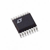
LTC1875EGN Linear Technology, LTC1875EGN Datasheet

LTC1875EGN
Specifications of LTC1875EGN
Available stocks
Related parts for LTC1875EGN
LTC1875EGN Summary of contents
Page 1
... Schottky diode. Low output voltages are easily supported with a 0.8V feedback reference voltage. The LTC1875 is available in a 16-lead SSOP package. , LTC and LT are registered trademarks of Linear Technology Corporation. Burst Mode is a registered trademark of Linear Technology Corporation ...
Page 2
... OSC f > f PPLIN SOC I = 100mA – 100mA 0.7V, Duty Cycle < RUN INFORMATION ORDER PART TOP VIEW NUMBER 16 PLL_LPF LTC1875EGN 15 SYNC/MODE 14 PGOOD SWP2 GN PART 11 SWN2 MARKING 10 PGND2 9 PV IN2 1875 GN PACKAGE = 110 MIN TYP MAX 8 60 0.784 0.80 0.816 0.740 ...
Page 3
ELECTRICAL CHARACTERISTICS temperature range, otherwise specifications are T SYMBOL PARAMETER V RUN Threshold RUN I RUN Input Current RUN Note 1: Absolute Maximum Ratings are those values beyond which the life of a device may be impaired. Note 2: The ...
Page 4
LTC1875 W U TYPICAL PERFOR A CE CHARACTERISTICS Output Voltage vs Load Current 1.84 1.82 1.80 1.78 1.76 1.74 Burst Mode OPERATION 1. 3. 4.7 H 1.70 0 500 1000 LOAD CURRENT (mA) Efficiency vs ...
Page 5
W U TYPICAL PERFOR A CE CHARACTERISTICS Load Step Response (Pulse Skipping Mode) V OUT 100mV/DIV I L 1A/DIV I TH 1V/DIV 100 s/DIV ...
Page 6
LTC1875 CTIO S SGND (Pin 1): Signal Ground Pin. RUN/SS (Pin 2): Combination of Soft-Start and Run Control Inputs. Forcing this pin below 0.7V shuts down the device. In shutdown all functions are disabled and ...
Page 7
W BLOCK DIAGRA LTC1875 1875f 7 ...
Page 8
LTC1875 U OPERATIO (Refer to Block Diagram) Main Control Loop The LTC1875 uses a constant frequency, current mode step-down architecture. Both the top MOSFET and syn- chronous bottom MOSFET switches are internal. During normal operation, the internal top power MOSFET ...
Page 9
U OPERATIO (Refer to Block Diagram) Power Good Indicator The power good function monitors the output voltage in all modes of operation. Its open-drain output is pulled low when the output voltage is not within 7.5% of its nomi- nally ...
Page 10
LTC1875 U OPERATIO Slope Compensation and Inductor Peak Current Slope compensation is required in order to prevent sub- harmonic oscillation at high duty cycles accom- plished by internally adding a compensating ramp to the inductor current signal at ...
Page 11
U U APPLICATIO S I FOR ATIO C and C Selection IN OUT In continuous mode, the source current of the top MOSFET is a trapezoidal waveform of duty cycle V prevent large voltage transients, a low ESR input capacitor ...
Page 12
LTC1875 U U APPLICATIO S I FOR ATIO 0.8V V OUT V FB LTC1875 SGND Figure 4. Setting the LTC1875 Output Voltage Phase-Locked Loop and Frequency Synchronization The LTC1875 has an internal voltage-controlled oscillator and phase detector comprising a phase-locked ...
Page 13
U U APPLICATIO S I FOR ATIO Efficiency Considerations The efficiency of a switching regulator is equal to the output power divided by the input power times 100 often useful to analyze individual losses to determine what is ...
Page 14
LTC1875 U U APPLICATIO S I FOR ATIO To avoid the LTC1875 from exceeding the maximum junction temperature, the user will need to do some thermal analysis. The goal of the thermal analysis is to determine whether the power dissipated ...
Page 15
U U APPLICATIO S I FOR ATIO PC Board Layout Checklist As with all high frequency switchers, when considering layout, care must be taken in order to achieve optimal electrical, thermal and noise performance. Figure sample of ...
Page 16
LTC1875 U U APPLICATIO S I FOR ATIO 4. Place the small-signal components away from high frequency switching nodes. In the layout shown in Figure 8, all of the small-signal components have been placed on one side of the IC ...
Page 17
U U APPLICATIO S I FOR ATIO C SVIN 0 100k POWER GOOD 0 47pF C C2 220pF R C 150k BOLD LINES INDICATE HIGH CURRENT PATHS C , ...
Page 18
LTC1875 U TYPICAL APPLICATIO Single Li-Ion to 1.8V/1.5A Regulator Using All Ceramic Capacitors C SVIN 0 100k POWER GOOD 0 47pF C C2 220pF R C 150k BOLD LINES ...
Page 19
... FLASH SHALL NOT EXCEED 0.010" (0.254mm) PER SIDE Information furnished by Linear Technology Corporation is believed to be accurate and reliable. However, no responsibility is assumed for its use. Linear Technology Corporation makes no represen- tation that the interconnection of its circuits as described herein will not infringe on existing patent rights. ...
Page 20
... OUT LTC3430 60V, 2.75A (I ), 200kHz High Efficiency Step-Down OUT DC/DC Converter LTC3440 600mA (I ), 2MHz Synchronous Buck-Boost OUT DC/DC Converter ThinSOT is a trademark of Linear Technology Corporation. Linear Technology Corporation 20 1630 McCarthy Blvd., Milpitas, CA 95035-7417 (408) 432-1900 FAX: (408) 434-0507 R SVIN 10 C SVIN ...


