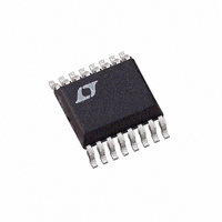
LTC1875EGN Linear Technology, LTC1875EGN Datasheet - Page 8

LTC1875EGN
Manufacturer Part Number
LTC1875EGN
Description
IC REG STEP-DWN SYNC 1.5A 16SSOP
Manufacturer
Linear Technology
Type
Step-Down (Buck)r
Datasheet
1.LTC1875EGNPBF.pdf
(20 pages)
Specifications of LTC1875EGN
Internal Switch(s)
Yes
Synchronous Rectifier
Yes
Number Of Outputs
1
Voltage - Output
0.8 ~ 6 V
Current - Output
1.5A
Frequency - Switching
550kHz
Voltage - Input
2.65 ~ 6 V
Operating Temperature
-40°C ~ 85°C
Mounting Type
Surface Mount
Package / Case
16-SSOP
Lead Free Status / RoHS Status
Contains lead / RoHS non-compliant
Power - Output
-
Available stocks
Company
Part Number
Manufacturer
Quantity
Price
Company:
Part Number:
LTC1875EGN
Manufacturer:
LT
Quantity:
10 000
OPERATIO
LTC1875
Main Control Loop
The LTC1875 uses a constant frequency, current mode
step-down architecture. Both the top MOSFET and syn-
chronous bottom MOSFET switches are internal. During
normal operation, the internal top power MOSFET is
turned on each cycle when the oscillator sets the RS latch,
and turned off when the current comparator, I
the RS latch. The peak inductor current at which I
turns the top MOSFET off is controlled by the voltage on
the I
the load current increases, it causes a slight decrease in
the feedback voltage, V
reference, which, in turn, causes the I
crease until the average inductor current matches the new
load current. While the top MOSFET is off, the bottom
MOSFET is turned on until either the inductor current
starts to reverse direction or the next clock cycle begins.
Comparator OVDET guards against transient overshoots
> 7.5% by turning the main switch off and keeping it off
until the fault is removed.
Burst Mode Operation
The LTC1875 is capable of Burst Mode operation in which
the internal power MOSFETs operate intermittently based
on load demand. To enable Burst Mode operation, simply
tie the SYNC/MODE pin to SV
(V
and enable PWM pulse skipping mode, connect the SYNC/
MODE pin to SGND. In this mode, the efficiency is lower at
light loads but becomes comparable to Burst Mode opera-
tion when the output load exceeds 100mA. The advantage
of pulse skipping mode is lower output ripple.
When the converter is in Burst Mode operation, the peak
current of the inductor is set to approximately 400mA,
even though the voltage at the I
value. The voltage at the I
average current is greater than the load requirement. As
8
SYNC/MODE
TH
pin, which is the output of error amplifier EA. When
> 1.5V). To disable Burst Mode operation
U
(Refer to Block Diagram)
FB
TH
, relative to the 0.8V internal
pin drops when the inductor’s
IN
or connect it to a logic high
TH
pin indicates a lower
TH
voltage to in-
COMP
, resets
COMP
the I
BURST comparator trips, turning off both power MOSFETs.
The I
amplifier and held 0.65V above ground.
In sleep mode, both power MOSFETs are held off and the
internal circuitry is partially turned off, reducing the quies-
cent current to 15 A. The load current is now being
supplied from the output capacitor. When the output
voltage drops, the I
EA amplifier and the top MOSFET is again turned on and
this process repeats.
Soft-Start/Run Function
The RUN/SS pin provides a soft-start function and a
means to shut down the LTC1875. Soft-start reduces the
input current surge by gradually increasing the regulator’s
maximum output current. This pin can also be used for
power supply sequencing.
Pulling the RUN/SS pin below 0.7V shuts down the
LTC1875, which then draws < 1 A current from the sup-
ply. This pin can be driven directly from logic circuits as
shown in Figure 1. It is recommended that this pin is driven
to V
current flowing out of this pin. Soft-start action is accom-
plished by connecting an external RC network to the RUN/
SS pin as shown in Figure 1. The LTC1875 actively pulls
the RUN/SS pin to ground under low input supply voltage
conditions.
IN
TH
TH
during normal operation. Note that there is no
pin is then disconnected from the output of the EA
voltage drops below approximately 0.45V, the
3.3V OR 5V
Figure 1. RUN/SS Pin Interfacing
TH
*ZETEX BAT54
0.32V
pin reconnects to the output of the
D1*
V
IN
R
SS
1875 F01
C
SS
RUN/SS
1875f


