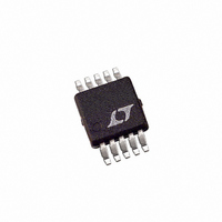
LTC3809EMSE-1 Linear Technology, LTC3809EMSE-1 Datasheet - Page 19

LTC3809EMSE-1
Manufacturer Part Number
LTC3809EMSE-1
Description
IC CTRLR DC/DC SYNC 10-MSOP
Manufacturer
Linear Technology
Type
Step-Down (Buck)r
Datasheet
1.LTC3809EMSE-1PBF.pdf
(24 pages)
Specifications of LTC3809EMSE-1
Internal Switch(s)
No
Synchronous Rectifier
Yes
Number Of Outputs
1
Voltage - Output
0.6 ~ 9.8 V
Current - Output
1A
Frequency - Switching
550kHz
Voltage - Input
2.75 ~ 9.8 V
Operating Temperature
-40°C ~ 85°C
Mounting Type
Surface Mount
Package / Case
10-MSOP Exposed Pad, 10-HMSOP, 10-eMSOP
Lead Free Status / RoHS Status
Contains lead / RoHS non-compliant
Power - Output
-
Available stocks
Company
Part Number
Manufacturer
Quantity
Price
Company:
Part Number:
LTC3809EMSE-1
Manufacturer:
LT
Quantity:
10 000
Company:
Part Number:
LTC3809EMSE-1#PBF
Manufacturer:
Linear Technology
Quantity:
135
APPLICATIONS INFORMATION
If the duty cycle falls below what can be accommodated
by the minimum on-time, the LTC3809-1 will begin to skip
cycles (unless forced continuous mode is selected). The
output voltage will continue to be regulated, but the ripple
current and ripple voltage will increase. The minimum on-
time for the LTC3809-1 is typically about 210ns. However,
as the peak sense voltage (I
the minimum on-time gradually increases up to about
260ns. This is of particular concern in forced continuous
applications with low ripple current at light loads. If forced
continuous mode is selected and the duty cycle falls below
the minimum on time requirement, the output will be
regulated by overvoltage protection.
Effi ciency Considerations
The effi ciency of a switching regulator is equal to the output
power divided by the input power times 100%. It is often
useful to analyze individual losses to determine what is
limiting effi ciency and which change would produce the
most improvement. Effi ciency can be expressed as:
where L1, L2, etc. are the individual losses as a percentage
of input power.
Although all dissipative elements in the circuit produce
losses, four main sources usually account for most of
the losses in LTC3809-1 circuits: 1) LTC3809-1 DC bias
current, 2) MOSFET gate-charge current, 3) I
and 4) transition losses.
1) The V
in the Electrical Characteristics, which excludes MOSFET
driver currents. V
increases with V
2) MOSFET gate-charge current results from switching
the gate capacitance of the power MOSFET. Each time a
MOSFET gate is switched from low to high to low again,
a packet of charge dQ moves from V
resulting dQ/dt is a current out of V
much larger than the DC supply current. In continuous
mode, I
Effi ciency = 100% – (L1 + L2 + L3 + …)
GATECHG
IN
(pin) current is the DC supply current, given
= f • Q
IN
IN
.
current results in a small loss that
P
.
L(PEAK)
• R
IN
, which is typically
DS(ON)
IN
to ground. The
) decreases,
2
R losses
3) I
MOSFETs, inductor and/or sense resistor. In continuous
mode, the average output current fl ows through L but
is “chopped” between the top P-channel MOSFET and
the bottom N-channel MOSFET. The MOSFET R
multiplied by duty cycle can be summed with the resistance
of L to obtain I
4) Transition losses apply to the external MOSFET and
increase with higher operating frequencies and input
voltages. Transition losses can be estimated from:
Other losses, including C
and inductor core losses, generally account for less than
2% total additional loss.
Checking Transient Response
The regulator loop response can be checked by looking
at the load transient response. Switching regulators take
several cycles to respond to a step in load current. When
a load step occurs, V
equal to (ΔI
ries resistance of C
discharge C
by the regulator to return V
During this recovery time, V
overshoot or ringing that would indicate a stability problem.
OPTI-LOOP compensation allows the transient response
to be optimized over a wide range of output capacitance
and ESR values.
The I
the dominant pole-zero loop compensation.
The I
fi rst page of this data sheet will provide adequate compen-
sation for most applications. The values can be modifi ed
slightly (from 0.2 to 5 times their suggested values) to
optimize transient response once the fi nal PC layout is done
and the particular output capacitor type and value have
been determined. The output capacitor needs to be decided
upon because the various types and values determine the
loop feedback factor gain and phase. An output current
Transition Loss = 2 • V
2
R losses are calculated from the DC resistances of the
TH
TH
external components showed in the fi gure on the
series R
LOAD
OUT
2
R losses.
generating a feedback error signal used
C
) • (ESR), where ESR is the effective se-
-C
OUT
C
OUT
fi lter (see Functional Diagram) sets
. ΔI
IN
immediately shifts by an amount
IN
and C
LOAD
2
OUT
• I
OUT
O(MAX)
OUT
to its steady-state value.
also begins to charge or
can be monitored for
ESR dissipative losses
LTC3809-1
• C
RSS
• f
19
DS(ON)
38091fc


