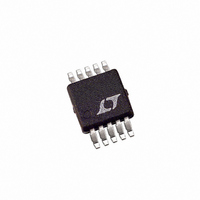
LTC3809EMSE-1 Linear Technology, LTC3809EMSE-1 Datasheet - Page 12

LTC3809EMSE-1
Manufacturer Part Number
LTC3809EMSE-1
Description
IC CTRLR DC/DC SYNC 10-MSOP
Manufacturer
Linear Technology
Type
Step-Down (Buck)r
Datasheet
1.LTC3809EMSE-1PBF.pdf
(24 pages)
Specifications of LTC3809EMSE-1
Internal Switch(s)
No
Synchronous Rectifier
Yes
Number Of Outputs
1
Voltage - Output
0.6 ~ 9.8 V
Current - Output
1A
Frequency - Switching
550kHz
Voltage - Input
2.75 ~ 9.8 V
Operating Temperature
-40°C ~ 85°C
Mounting Type
Surface Mount
Package / Case
10-MSOP Exposed Pad, 10-HMSOP, 10-eMSOP
Lead Free Status / RoHS Status
Contains lead / RoHS non-compliant
Power - Output
-
Available stocks
Company
Part Number
Manufacturer
Quantity
Price
Company:
Part Number:
LTC3809EMSE-1
Manufacturer:
LT
Quantity:
10 000
Company:
Part Number:
LTC3809EMSE-1#PBF
Manufacturer:
Linear Technology
Quantity:
135
APPLICATIONS INFORMATION
LTC3809-1
The typical LTC3809-1 application circuit is shown in Figure
8. External component selection for the controller is driven
by the load requirement and begins with the selection of
the inductor and the power MOSFETs.
Power MOSFET Selection
The LTC3809-1’s controller requires two external power
MOSFETs: a P-channel MOSFET for the topside (main)
switch and a N-channel MOSFET for the bottom (synchro-
nous) switch. The main selection criteria for the power
MOSFETs are the breakdown voltage V
voltage V
capacitance C
charge Q
The gate drive voltage is the input supply voltage. Since
the LTC3809-1 is designed for operation down to low input
voltages, a sublogic level MOSFET (R
V
this voltage. When these MOSFETs are used, make sure that
the input supply to the LTC3809-1 is less than the absolute
maximum MOSFET V
The P-channel MOSFET’s on-resistance is chosen based
on the required load current. The maximum average load
current I
minus half the peak-to-peak ripple current I
LTC3809-1’s current comparator monitors the drain-to-
source voltage V
is sensed between the V
current is limited by the current threshold, set by the voltage
on the I
the I
current sense threshold ΔV
125mV when IPRG is fl oating (85mV when IPRG is tied
low; 204mV when IPRG is tied high).
The output current that the LTC3809-1 can provide is
given by:
12
GS
I
OUT MAX
TH
= 2.5V) is required for applications that work close to
pin is internally clamped, which limits the maximum
(
TH
OUT(MAX)
G
GS(TH)
.
pin, of the current comparator. The voltage on
)
=
RSS
Δ
, on-resistance R
DS
V
, turn-off delay t
R
SENSE MAX
is equal to the peak inductor current
of the top P-channel MOSFET, which
DS ON
GS
(
IN
(
rating, which is typically 8V.
)
and SW pins. The peak inductor
SENSE(MAX)
)
–
I
RIPPLE
DS(ON)
D(OFF)
2
DS(ON)
BR(DSS)
, reverse transfer
and the total gate
to approximately
guaranteed at
RIPPLE
, threshold
. The
where I
(see Inductor Value Calculation).
A reasonable starting point is setting ripple current I
to be 40% of I
yields:
However, for operation above 20% duty cycle, slope
compensation has to be taken into consideration to select
the appropriate value of R
amount of load current:
where SF is a scale factor whose value is obtained from
the curve in Figure 1.
These must be further derated to take into account the
signifi cant variation in on-resistance with temperature. The
following equation is a good guide for determining the re-
quired R
allowing some margin for variations in the LTC3809-1 and
external component values:
The ρ
variation in on-resistance, which is typically about 0.4%/°C,
as shown in Figure 2. Junction-to-case temperature T
about 10°C in most applications. For a maximum ambi-
ent temperature of 70°C, using ρ
equation is a reasonable choice.
The N-channel MOSFET’s on resistance is chosen based
on the short-circuit current limit (I
1’s short-circuit current limit comparator monitors the
drain-to-source voltage V
MOSFET, which is sensed between the GND and SW pins.
R
DS ON MAX
R
R
(
DS ON MAX
DS ON MAX
T
is a normalizing term accounting for the temperature
(
(
RIPPLE
)
DS(ON)MAX
)
)
=
is the inductor peak-to-peak ripple current
OUT(MAX)
5
6
=
=
•
6
6
5
5
Δ
at 25°C (manufacturer’s specifi cation),
•
• . •
V
I
SF
0 9
OUT MAX
SENSE MAX
. Rearranging the above equation
•
(
Δ
SF
DS(ON)
DS
(
V
I
OUT MAX
SENSE MAX
•
)
I
Δ
of the bottom N-channel
OUT MAX
)
(
V
for Duty C
to provide the required
SENSE MAX
80°C
(
(
)
SC
~ 1.3 in the above
)
(
)
). The LTC3809-
•
ρ ρ
T
y y cle < 20%
)
RIPPLE
38091fc
JC
is


