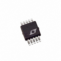
LTC3809EMSE-1 Linear Technology, LTC3809EMSE-1 Datasheet - Page 13

LTC3809EMSE-1
Manufacturer Part Number
LTC3809EMSE-1
Description
IC CTRLR DC/DC SYNC 10-MSOP
Manufacturer
Linear Technology
Type
Step-Down (Buck)r
Datasheet
1.LTC3809EMSE-1PBF.pdf
(24 pages)
Specifications of LTC3809EMSE-1
Internal Switch(s)
No
Synchronous Rectifier
Yes
Number Of Outputs
1
Voltage - Output
0.6 ~ 9.8 V
Current - Output
1A
Frequency - Switching
550kHz
Voltage - Input
2.75 ~ 9.8 V
Operating Temperature
-40°C ~ 85°C
Mounting Type
Surface Mount
Package / Case
10-MSOP Exposed Pad, 10-HMSOP, 10-eMSOP
Lead Free Status / RoHS Status
Contains lead / RoHS non-compliant
Power - Output
-
Available stocks
Company
Part Number
Manufacturer
Quantity
Price
Company:
Part Number:
LTC3809EMSE-1
Manufacturer:
LT
Quantity:
10 000
Company:
Part Number:
LTC3809EMSE-1#PBF
Manufacturer:
Linear Technology
Quantity:
135
APPLICATIONS INFORMATION
The short-circuit current sense threshold ΔV
approximately 90mV when IPRG is fl oating (60mV when
IPRG is tied low; 150mV when IPRG is tied high). The
on-resistance of N-channel MOSFET is determined by:
The short-circuit current limit (I
than the I
with the peak current sensing loop. On the other hand,
in order to prevent the MOSFETs from excessive heating
and the inductor from saturation, I
smaller than the minimum value of their current ratings.
A reasonable range is:
Therefore, the on-resistance of N-channel MOSFET should
be chosen within the following range:
where ΔV
fl oated, tied to GND or V
The power dissipated in the MOSFET strongly depends
on its respective duty cycles and load current. When the
LTC3809-1 is operating in continuous mode, the duty
cycles for the MOSFETs are:
I
R
I
OUT(MAX)
RATING MIN
DS ON MAX
Δ
(
V
OUT(MAX)
SC
SC
)
(
2.0
1.0
0.5
1.5
< I
is 90mV, 60mV or 150mV with IPRG being
0
–50
Figure 2. R
)
=
SC(PEAK)
<
I
R
SC PEAK
with some margin to avoid interfering
DS ON
Δ
JUNCTION TEMPERATURE (°C)
(
V
(
0
SC
DS(ON)
< I
IN
)
)
<
RATING(MIN)
respectively.
I
OUT MAX
50
vs Temperature
Δ
SC(PEAK)
V
(
SC
100
)
SC(PEAK)
) should be larger
38091 F02
150
should be
SC
is set
The MOSFET power dissipations at maximum output
current are:
Both MOSFETs have I
includes an additional term for transition losses, which are
largest at high input voltages. The bottom MOSFET losses
are greatest at high input voltage or during a short-circuit
when the bottom duty cycle is 100%.
The LTC3809-1 utilizes a non-overlapping, anti-shoot-
through gate drive control scheme to ensure that the
P- and N-channel MOSFETs are not turned on at the same
time. To function properly, the control scheme requires
that the MOSFETs used are intended for DC/DC switching
applications. Many power MOSFETs, particularly P-channel
MOSFETs, are intended to be used as static switches and
therefore are slow to turn on or off.
Reasonable starting criteria for selecting the P-channel
MOSFET are that it must typically have a gate charge (Q
less than 25nC to 30nC (at 4.5V
(t
to differences in test and specifi cation methods of various
MOSFET manufacturers, and in the variations in Q
t
ultimately should be evaluated in the actual LTC3809-1
application circuit to ensure proper operation.
Shoot-through between the P-channel and N-channel
MOSFETs can most easily be spotted by monitoring the
input supply current. As the input supply voltage increases,
if the input supply current increases dramatically, then the
likely cause is shoot-through. Note that some MOSFETs
D(OFF)
D(OFF)
Bottom N-
P
P
Top P-Channel Duty Cycle =
BOT
TOP
with gate drive (V
) of less than approximately 140ns. However, due
=
=
•
V
V
I
V
OUT
IN
OUT MAX
IN
C C hannel Duty Cycle =
–
V
IN
(
V
•
OUT
I
OUT MAX
)
•
2
(
•
IN
R losses and the P
C
I
OUT MAX
) voltage, the P-channel MOSFET
RSS
)
2
(
•
•
ρ
f
GS
V
T
)
V
2
OUT
) and a turn-off delay
•
LTC3809-1
IN
•
V
R
ρ
IN
DS ON
T
− V
V
(
•
IN
R
OUT
TOP
)
DS ON
+
(
2
equation
13
•
)
G
V
38091fc
IN
and
2
G
)


