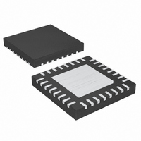
MAX5099ATJ+ Maxim Integrated Products, MAX5099ATJ+ Datasheet - Page 15

MAX5099ATJ+
Manufacturer Part Number
MAX5099ATJ+
Description
IC CONV BUCK SYNC DL 32TQFN-EP
Manufacturer
Maxim Integrated Products
Type
Step-Down (Buck)r
Datasheet
1.MAX5099ATJ.pdf
(27 pages)
Specifications of MAX5099ATJ+
Internal Switch(s)
Both
Synchronous Rectifier
Yes
Number Of Outputs
2
Voltage - Output
0.8 ~ 17.1 V
Current - Output
1A, 2A
Frequency - Switching
200kHz ~ 2.2MHz
Voltage - Input
4.5 ~ 19 V
Operating Temperature
-40°C ~ 125°C
Mounting Type
Surface Mount
Package / Case
32-TQFN Exposed Pad
Power - Output
2.76W
Output Voltage
5.2 V
Output Current
2 A
Input Voltage
5.2 V to 19 V
Supply Current
4.2 mA
Switching Frequency
1.9 MHz
Mounting Style
SMD/SMT
Maximum Operating Temperature
+ 125 C
Minimum Operating Temperature
- 40 C
Lead Free Status / RoHS Status
Lead free / RoHS Compliant
The MAX5099 provide an input (ON/OFF) to turn on and
off the external load-dump protection MOSFET. Drive
ON/OFF high for normal operation. Drive ON/OFF low to
turn off the external n-channel load-dump protection
MOSFET and reduce the supply current to 7μA (typ).
When ON/OFF is driven low, both converters are also
turned off, and the PGOOD_ outputs are driven, low. V+
will be self-discharged through the converters’ output
currents and the IC supply current.
The internal oscillator generates the 180° out-of-phase
clock signal required by each regulator. The switching
frequency of each converter (f
from 200kHz to 2.2MHz using a single 1% resistor at
R
With dual-synchronized out-of-phase operation, the
MAX5099’s internal MOSFETs turn on 180° out-of-
phase. The instantaneous input current peaks of both
regulators do not overlap, resulting in reduced RMS rip-
ple current and input-voltage ripple. This reduces the
required input capacitor ripple current rating, allows for
fewer or less expensive capacitors, and reduces
shielding requirements for EMI.
The main oscillator can be synchronized to the system
clock by applying an external clock (f
The f
ing frequency of an individual converter. Use a TTL logic
signal for the external clock with at least a 100ns pulse
width. R
chronization. Program the internal oscillator frequency to
have f
nized if the SYNC frequency f
range ±20%.
Short SYNC to SGND if unused.
All internal control circuitry operates from an internally
regulated nominal voltage of 5.2V (V
voltages (V+) of 5.2V to 19V, V
OSC
SYNC
. See the Setting the Switching Frequency section.
SW
Dual, 2.2MHz, Automotive Synchronous Buck
OSC
= 1/2 f
frequency must be twice the required operat-
is still required when using external syn-
Converter with 80V Load-Dump Protection
SYNC
Internal Linear Regulator (V
______________________________________________________________________________________
. The device is properly synchro-
Synchronization (SYNC)
Out-of-Phase Operation
L
Internal Oscillator/
Input Voltage (V+)/
SYNC
is regulated to 5.2V. At
SW
) is programmable
L
varies within the
). At higher input
SYNC
) at SYNC.
ON/OFF
L
)
5.2V or below, the internal linear regulator operates in
dropout mode, where V
load on V
reduce V
threshold. Do not use V
For input voltages less than 5.5V, connect V+ and V
together. The load on V
frequency of converter 1 and converter 2. See the V
Output Voltage vs. Converter Switching Frequency
graph in the Typical Operating Characteristics . For
input voltage ranges higher than 5.5V, disconnect V
from V+.
Bypass V+ to SGND with a 1μF or greater ceramic
capacitor placed close to the MAX5099. Bypass V
a low-ESR 4.7μF ceramic capacitor to SGND.
The MAX5099 includes an undervoltage lockout with
hysteresis and a power-on-reset circuit for converter
turn-on and monotonic rise of the output voltage. The
falling UVLO threshold is internally set to 4.1V (typ) with
180mV hysteresis. Hysteresis at UVLO eliminates “chat-
tering” during startup. When V
internal MOSFET switches are turned off.
The MAX5099 digital soft-start reduces input inrush
currents and glitches at the input during turn-on. When
UVLO is cleared and EN_ is high, digital soft-start slow-
ly ramps up the internal reference voltage in 64 steps.
The total soft-start period is 4096 internal oscillator
switching cycles.
Driving EN_ low initiates digital soft-stop that slowly
ramps down the internal reference voltage in 64 steps.
The total soft-stop period is equal to the soft-start period.
To calculate the soft-start/soft-stop period, use the fol-
lowing equation:
where f
each converter’s switching frequency (FSEL_1 = V
OSC
L
L
, the dropout voltage can be high enough to
below the undervoltage-lockout (UVLO)
is the internal oscillator and f
t
SS
(
ms
L
L
L
)
to power external circuitry.
is proportional to the switching
follows V+. Depending on the
=
Undervoltage Lockout/
f
OSC
L
Soft-Start/Soft-Stop
4096
drops below UVLO, the
(
kHz
)
OSC
is twice
L
L
).
with
15
L
L
L


